SMT Assembly vs. Through-Hole: A Comparative Analysis for the 2026 PCB Manufacturing Landscape
SMT Assembly vs. Through-Hole: A Comparative Analysis for the 2026 PCB Manufacturing Landscape Introduction In the rapidly evolving landscape of electronics manufacturing, Surface Mount Technology (SM...
Introduction
In the rapidly evolving landscape of electronics manufacturing, Surface Mount Technology (SMT) and Through-Hole Technology (THT) continue to be pivotal methods for Printed Circuit Board (PCB) assembly. As we approach 2026, understanding the nuances between these two technologies is crucial for engineers and manufacturers aiming to optimize design, efficiency, and performance. This comparative analysis delves into the intricacies of PCB layout rules, stackup design, signal integrity, and manufacturing considerations, providing a comprehensive guide to navigate the complexities of modern PCB manufacturing.
Technical Overview
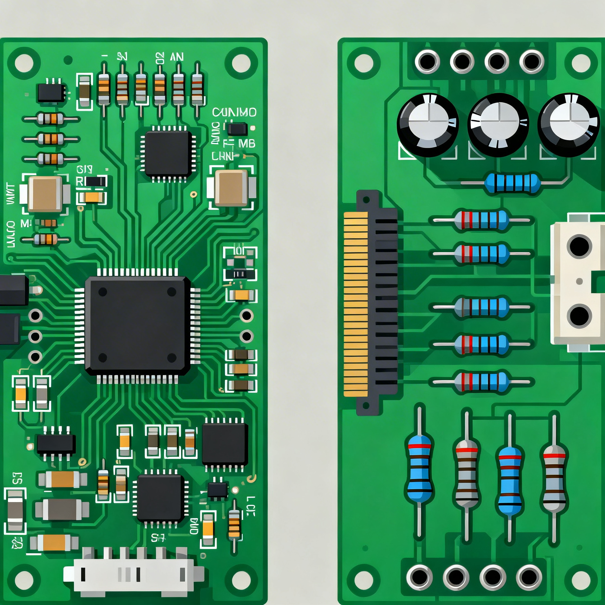
Surface Mount Technology (SMT) and Through-Hole Technology (THT) are fundamental to PCB assembly, each offering distinct advantages and challenges. SMT involves mounting components directly onto the surface of the PCB, allowing for more compact and lightweight designs. THT, on the other hand, involves inserting component leads through holes in the PCB, providing robust mechanical connections and reliability in harsh environments. Understanding the architectural principles of these technologies is essential for selecting the appropriate method based on project requirements, such as signal integrity, power handling, and mechanical stability.
As electronics continue to shrink in size while increasing in complexity, the choice between SMT and THT becomes a critical decision point. SMT is favored for high-density applications due to its ability to accommodate a greater number of components on a single board. THT remains relevant for applications requiring high mechanical strength and ease of inspection and repair. This technical overview sets the stage for exploring detailed specifications and practical implications of each technology, ensuring informed decision-making in PCB manufacturing.
Detailed Specifications
When designing PCBs, adherence to specific design rules is paramount to ensure functionality and manufacturability. Critical specifications include trace widths, spacing, via sizes, and clearances, which directly impact signal integrity and electrical performance. The following table outlines essential PCB design rules, serving as a guide for engineers to optimize their layouts for both SMT and THT applications.
| Design Parameter | SMT | Through-Hole |
|---|---|---|
| Minimum Trace Width | 0.1 mm | 0.3 mm |
| Minimum Trace Spacing | 0.1 mm | 0.3 mm |
| Minimum Via Diameter | 0.25 mm | 0.6 mm |
| Pad Size for ICs | 1.0 mm | 2.5 mm |
| Clearance to Edge | 0.2 mm | 0.5 mm |
| Component Height | 1.5 mm | 5.0 mm |
| Solder Mask Clearance | 0.05 mm | 0.1 mm |
| Annular Ring | 0.15 mm | 0.3 mm |
| Thermal Relief Spokes | 4 | 4 |
| Silkscreen Line Width | 0.1 mm | 0.2 mm |
Key Takeaways from the Specifications
The specifications outlined in the table highlight critical differences between SMT and THT design rules. SMT allows for finer trace widths and spacings, which facilitates higher component density and smaller PCB designs. This is ideal for modern electronics where space is at a premium. In contrast, THT requires larger traces and spacings, making it suitable for applications where durability and robustness are prioritized over miniaturization. Understanding these specifications is essential for engineers to make informed decisions about which technology best suits their design requirements, balancing factors like cost, performance, and manufacturability.
| Layer Stackup Configuration | Layers | Application |
|---|---|---|
| Single Layer | 1 | Simple, low-cost designs |
| Double Layer | 2 | Basic consumer electronics |
| Four Layer | 4 | Complex circuits with ground/power planes |
| Six Layer | 6 | High-speed, high-density designs |
| Eight Layer | 8 | Advanced communication devices |
| Ten Layer | 10 | High-performance computing |
| Twelve Layer | 12 | Server and data center applications |
Practical Implications
The choice of layer stackup configuration plays a critical role in the performance and functionality of a PCB. Single and double-layer boards are cost-effective and suited for simpler designs. As complexity increases, additional layers provide the necessary routing space and improve signal integrity by separating signal and power planes. High-speed and high-density applications, such as those found in communication and computing devices, benefit from multi-layer configurations, which enhance performance and reduce electromagnetic interference. Understanding the practical implications of each stackup option ensures optimal design and functionality for specific applications.
| Material | Dielectric Constant (Dk) | Loss Tangent (Df) |
|---|---|---|
| FR-4 | 4.5 | 0.02 |
| Rogers 4350B | 3.66 | 0.0037 |
| Rogers 4003C | 3.38 | 0.0027 |
| Isola FR408HR | 3.65 | 0.008 |
| Nelco N4000-13 | 3.7 | 0.009 |
| Panasonic Megtron 6 | 3.4 | 0.002 |
| Arlon 85N | 3.5 | 0.004 |
| DuPont Pyralux | 3.2 | 0.002 |
| Polyimide | 4.2 | 0.004 |
Application Guidelines
The selection of PCB materials significantly influences the board's electrical performance and thermal stability. FR-4 remains a popular choice for general-purpose applications due to its balance of performance and cost. For high-frequency applications, materials like Rogers 4350B and Panasonic Megtron 6 offer lower dielectric constants and loss tangents, enhancing signal integrity and reducing power losses. Polyimide and other advanced materials provide superior thermal stability, making them suitable for applications exposed to extreme temperatures. Engineers must carefully evaluate material properties to align with the specific performance requirements of their applications.
Design Considerations
Effective PCB design requires a meticulous approach to layout planning, component placement, and routing strategies. Engineers must consider factors such as signal integrity, thermal management, and manufacturability. For SMT designs, minimizing trace lengths and optimizing component placement can significantly enhance signal performance. In THT applications, ensuring adequate hole size and spacing is crucial for reliable soldering and mechanical stability. Adhering to IPC standards, such as IPC-2221 for design and IPC-A-610 for assembly, ensures that designs meet industry quality benchmarks. Collaboration with PCB manufacturers during the design phase can further refine layouts for manufacturability and cost-effectiveness.
Thermal management is another critical design consideration, particularly in high-power applications. Implementing thermal vias, heat sinks, and appropriate copper weights can mitigate heat buildup and prevent component failure. Signal integrity is paramount in high-speed designs, necessitating careful attention to impedance matching, controlled impedance routing, and minimizing electromagnetic interference. By integrating these design considerations, engineers can achieve robust, high-performance PCB designs that meet the demands of modern electronics.
Step-by-Step Implementation
To successfully implement a PCB design, a structured approach is essential. The following steps outline a comprehensive process from concept to production:
- Define Requirements: Clearly outline the project requirements, including performance, size, and cost constraints.
- Schematic Design: Develop a detailed schematic that captures all electrical connections and component specifications.
- PCB Layout: Translate the schematic into a PCB layout, optimizing component placement and routing for performance and manufacturability.
- Simulation and Validation: Use simulation tools to validate signal integrity, thermal performance, and power distribution.
- Prototype Fabrication: Collaborate with a PCB manufacturer to produce a prototype, ensuring adherence to design specifications.
- Assembly and Testing: Assemble the PCB, conduct thorough testing to verify functionality and performance.
- Design Iteration: Based on test results, iterate the design to address any issues or optimizations.
- Final Production: Once validated, proceed to full-scale production, ensuring quality control at each stage.
Each step is critical to the success of the PCB design and manufacturing process. By following a methodical approach, engineers can minimize errors, optimize performance, and ensure the final product meets all specifications.
Common Issues & Solutions
PCB design and manufacturing can present several challenges. Here are some common issues and their solutions:
- Signal Integrity Issues: Use controlled impedance routing and proper grounding techniques to mitigate signal degradation.
- Thermal Management Problems: Implement thermal vias and heat sinks to dissipate heat effectively.
- Manufacturing Defects: Collaborate with manufacturers to ensure designs are optimized for production, reducing defects.
- Component Misalignment: Use precise placement tools and guidelines to ensure accurate component positioning.
- Solder Joint Failures: Optimize soldering profiles and use appropriate pad sizes to enhance joint reliability.
By proactively addressing these issues, engineers can enhance the reliability and performance of their PCBs, reducing the risk of failure in the field.
Applications & Use Cases
PCBs utilizing SMT and THT technologies find applications across various industries. SMT is prevalent in consumer electronics, where compactness and efficiency are paramount. THT remains favored in industrial and automotive applications, where durability and reliability are critical. In telecommunications, multi-layer SMT boards support high-speed data transfer, while medical devices benefit from the precision and reliability of THT. By understanding the strengths and limitations of each technology, engineers can tailor their designs to meet specific application requirements.
Selection & Sourcing Guide
When selecting components and materials for PCB design, sourcing reliable suppliers is crucial. Platforms like IC Online provide a comprehensive database of components, ensuring access to high-quality parts that meet design specifications. Establishing strong supplier relationships can streamline the sourcing process, reduce lead times, and lower costs, ultimately contributing to the success of PCB projects.
FAQ
- What is the main advantage of SMT over THT? SMT allows for higher component density and smaller PCB designs, making it ideal for compact electronic devices.
- Why is THT still used in some applications? THT provides robust mechanical connections and is preferred in environments where durability and reliability are critical.
- How does layer stackup affect PCB performance? Additional layers provide more routing space and improve signal integrity, crucial for high-speed and high-density applications.
- What materials are best for high-frequency applications? Materials like Rogers 4350B and Panasonic Megtron 6, with low dielectric constants and loss tangents, are ideal for high-frequency applications.
- How can signal integrity be improved in PCB designs? Implementing controlled impedance routing and proper grounding techniques can enhance signal integrity.
- What are the key considerations for thermal management in PCBs? Using thermal vias, heat sinks, and appropriate copper weights can effectively manage heat in high-power applications.
- How can manufacturing defects be minimized? Collaborating with manufacturers during the design phase can optimize layouts for manufacturability, reducing defects.
- What role do IPC standards play in PCB design? IPC standards provide guidelines for design, assembly, and quality inspection, ensuring industry compliance and reliability.
- How important is component placement in PCB design? Precise component placement is crucial for minimizing trace lengths and optimizing performance, especially in SMT designs.
- What tools are used for PCB simulation and validation? Simulation tools like SPICE and thermal analysis software are used to validate signal integrity and thermal performance.
Conclusion
As we navigate the complexities of 2026 PCB manufacturing, the choice between SMT and THT remains pivotal. Each technology offers unique advantages suited to different applications, from compact consumer electronics to robust industrial systems. By understanding the design rules, stackup options, and material properties, engineers can make informed decisions that optimize performance and manufacturability. Through careful planning and collaboration with manufacturers, the potential of modern PCBs can be fully realized, driving innovation and efficiency in the electronics industry.