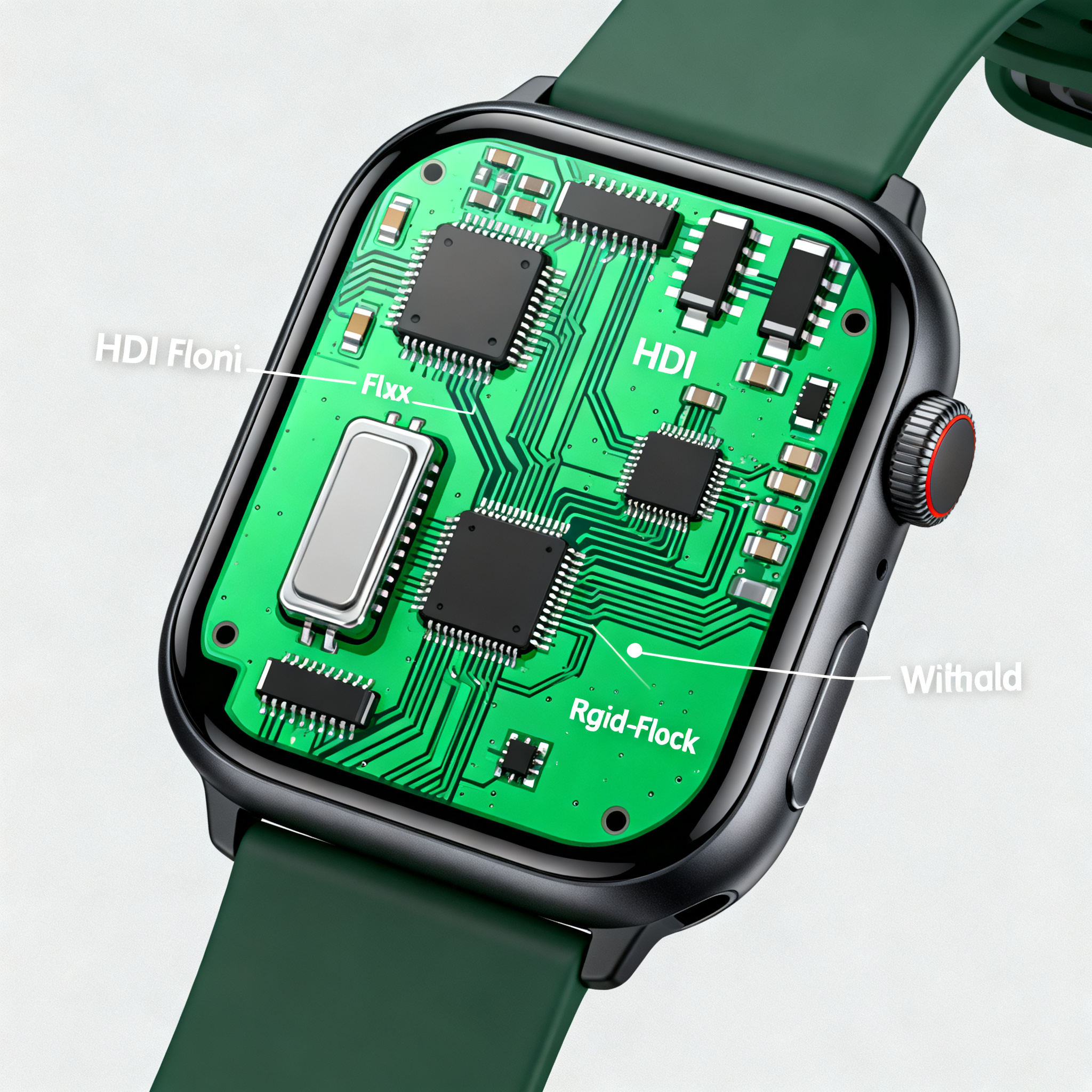
Smartwatch PCBA Assembly Services: A Comparison Guide to HDI, Flex, and Rigid-Flex Options for Miniaturized Wearables
The Shrinking Footprint and Rising Complexity of Smartwatch Electronics Smartwatch design has moved far beyond simple step counters. Today’s devices pack heart-rate monitors, SpO₂ sensors, GPS, NFC, h...
The Shrinking Footprint and Rising Complexity of Smartwatch Electronics
Smartwatch design has moved far beyond simple step counters. Today’s devices pack heart-rate monitors, SpO₂ sensors, GPS, NFC, haptic drivers, and bright AMOLED displays into a case that rarely exceeds 12 mm in thickness. The printed circuit board assembly (PCBA) at the core of this system must route dozens of high-speed signals, manage multiple power domains, and survive daily mechanical stress—all while leaving room for a battery that users expect to last a full day or more. Choosing the right PCB architecture is no longer a secondary decision; it defines the product’s performance envelope, assembly yield, and long-term field reliability.
Engineers and manufacturing buyers evaluating smartwatch PCBA assembly services quickly encounter three distinct platform options: high-density interconnect (HDI) rigid boards, flexible circuits (flex), and rigid-flex hybrids. Each brings a different balance of routing density, mechanical integration, and cost. The challenge is that a poor choice—or a poorly executed assembly—can lead to microvia cracking under thermal cycling, delamination in dynamic flex zones, or connector failures that drive up warranty returns. Industry standards such as IPC-A-610 (acceptability of electronic assemblies) and IPC-2221 (generic design standard) provide the quality and design benchmarks that separate robust wearable electronics from fragile prototypes. A partner like Nova PCBA, with dedicated experience in miniaturized wearable assemblies, can help navigate these requirements while keeping prototype and volume schedules on track.
This guide compares HDI, flex, and rigid-flex PCBA options specifically through the lens of smartwatch development. You’ll see how layer stackups, via structures, and materials differ, how the three architectures trade off in a real design matrix, and what to demand from an assembly supplier so that your next smartwatch build meets both form-factor goals and reliability targets.
From Microvias to Polyimide: How HDI, Flex, and Rigid-Flex PCBs Are Built
Before comparing architectures, it’s worth understanding what physically distinguishes an HDI rigid board from a flex circuit and how rigid‑flex combines the two. The differences start at the material level and cascade into via technology, trace geometry, and mechanical behavior.
HDI rigid PCBs use FR‑4 or high‑Tg glass‑epoxy laminates and rely on laser‑drilled microvias (typically 0.1 mm or smaller) to connect dense BGA escape patterns. Blind and buried vias free up routing channels on outer layers, allowing trace/space values down to 50 µm/50 µm on advanced processes. Stacked or staggered microvia structures are common, but they must follow aspect‑ratio rules from IPC‑2221 to avoid barrel cracks during reflow or thermal cycling. A typical smartwatch main board built as an HDI rigid PCB might use an 8‑layer stackup with two or three microvia layers, achieving high component density but remaining a flat, inflexible card that requires connectors or soldered flex tails to reach sensors and the display.
Flex PCBs replace rigid laminates with polyimide films and rolled‑annealed copper foils. Adhesiveless constructions dominate in wearables because they offer thinner profiles and better dynamic flex endurance. Vias in flex are usually mechanically drilled or laser‑formed, and while trace/space can approach 50 µm, the real advantage is the ability to form the circuit into a 3D shape inside the watch housing. A flex‑only smartwatch board might integrate the main processor, sensors, and battery connector on a single shaped polyimide substrate that wraps around the battery cavity, eliminating multiple connectors.
Rigid‑flex PCBs fuse rigid FR‑4 sections with polyimide flex layers in a single lamination cycle. The rigid areas carry components and connectors; the flex sections serve as integrated interconnects that bend once (“flex‑to‑install”) or repeatedly in a watch band. No‑flow prepregs and careful layer‑to‑layer registration are critical to prevent resin squeeze‑out into flex areas. Rigid‑flex stackups for smartwatches often combine 6‑8 rigid layers with 2‑4 flex layers, using blind and buried vias in the rigid zones and plated through‑holes at the rigid‑flex transition.
The table below captures typical parameter ranges for each architecture when applied to smartwatch‑scale designs.
| Parameter | HDI Rigid PCB | Flex PCB | Rigid‑Flex PCB | Notes for Smartwatch Design |
|---|---|---|---|---|
| Typical layer count | 6–10 layers | 2–8 layers | 6–12 total (rigid + flex) | Higher counts increase cost; rigid‑flex often uses 8 rigid + 2 flex layers. |
| Minimum trace/space | 50/50 µm (advanced: 40/40 µm) | 50/50 µm (75/75 µm for dynamic areas) | 50/50 µm on rigid, 75/75 µm on flex | Fine lines demand laser direct imaging and tight process control. |
| Minimum via diameter (laser) | 0.10 mm (microvia) | 0.15 mm | 0.10 mm (rigid), 0.15 mm (flex) | Microvia aspect ratio ≤ 1:1 per IPC‑2221; staggered preferred for reliability. |
| Finished board thickness | 0.6–1.0 mm | 0.12–0.30 mm | 0.8–1.2 mm (rigid zones) | Thinner flex improves bend radius but reduces component mounting stiffness. |
| Bend radius (dynamic) | N/A | ≥ 10× thickness (rolled‑annealed Cu) | ≥ 10× flex thickness | IPC‑2223 guidelines; dynamic flex life > 10M cycles achievable with proper design. |
| Typical dielectric material | FR‑4, high‑Tg FR‑4 | Polyimide (adhesiveless) | FR‑4 + polyimide, no‑flow prepreg | Adhesiveless flex reduces thickness and improves bend endurance. |
| Component mounting | Both sides; fine‑pitch BGA | One side preferred; stiffeners for BGA | Rigid sections: both sides; flex: passives only | Polyimide stiffeners or rigid islands support 0.4 mm‑pitch BGAs on flex. |
| Typical smartwatch use | Main logic board with connectors | Sensor flex, button flex, display interconnect | Integrated main board + band flex, or folded 3D assembly | Rigid‑flex often eliminates 2–4 board‑to‑board connectors. |
These numbers are not theoretical limits; they represent what experienced PCB fabricators and assembly houses routinely deliver for consumer wearable volumes. The key takeaway is that HDI rigid boards push density but remain planar, flex circuits enable 3D integration at the cost of component mounting complexity, and rigid‑flex merges the best of both while demanding tighter process control. The next section maps these characteristics onto the specific trade‑offs you face when designing a smartwatch.
HDI vs. Flex vs. Rigid‑Flex: Which PCB Architecture Fits Your Smartwatch Design?
Smartwatch product teams rarely have the luxury of choosing a PCB architecture in isolation. The decision is shaped by the industrial design (ID), sensor placement, antenna clearance, battery size, and assembly test strategy. The comparison matrix below evaluates the three architectures across the metrics that matter most in a wearable project.
| Metric | HDI Rigid PCB + Flex Interconnects | Flex‑Only PCB | Rigid‑Flex PCB | Selection Guidance for Smartwatches |
|---|---|---|---|---|
| Design density (components/cm²) | Very high; 0.35 mm‑pitch BGAs routable with microvias | Moderate; limited to one‑side component placement without stiffeners | High on rigid islands; flex zones carry only passives | HDI rigid or rigid‑flex wins for processor‑dense boards; flex‑only suits sensor sub‑assemblies. |
| Mechanical integration | Requires board‑to‑board connectors or hot‑bar soldered flex tails; adds Z‑height and assembly steps | Excellent; circuit can conform to curved housings and wrap around battery | Excellent; rigid sections lock into housing, flex sections fold naturally; no connectors in signal path | Rigid‑flex eliminates 2–4 connectors, reducing stack‑up height by 0.8–1.5 mm and removing a common failure point. |
| Assembly complexity | Multiple sub‑assemblies; connector mating requires precision fixtures; potential for coplanarity issues | Single‑piece assembly but needs pallets for SMT; fine‑pitch components require stiffeners | Single‑piece assembly; rigid zones can be processed like standard boards; flex areas need support during reflow | Rigid‑flex simplifies final assembly but demands experienced SMT partners who can handle mixed rigid‑flex panels. |
| Cost at prototype stage (100 units) | Moderate; multiple simple boards plus connectors and assembly labor | Lower tooling cost; higher per‑unit assembly cost due to pallets | Higher bare‑board NRE; single‑piece assembly reduces labor | Rigid‑flex prototypes cost 1.5–2× more than rigid‑plus‑connector solutions; the gap narrows above 10k units. |
| Cost at volume (>10k units) | Total system cost can be higher due to connector BOM and multiple assembly/test cycles | Competitive if design is simple; limited for high‑density logic | Often lower total system cost because connectors, FPCs, and associated assembly steps are eliminated | For feature‑rich smartwatches, rigid‑flex frequently delivers the lowest system cost at scale, despite higher bare‑board price. |
| Reliability (mechanical) | Connectors are the weak link; fretting corrosion and intermittent opens under shock/vibration | Excellent dynamic flex life if bend radius rules are followed; no connectors to fail | Excellent; integrated flex eliminates connector failures; rigid‑flex transitions must be designed to avoid stress risers | Rigid‑flex offers the highest overall reliability for products that experience daily wear and occasional drops. |
| Signal integrity | Controlled impedance possible on rigid layers; connectors introduce discontinuities | Impedance control more challenging due to thin dielectrics; reference plane continuity needed across bends | Seamless impedance control from rigid to flex; no connector stubs; ideal for MIPI DSI and USB 3.x | Rigid‑flex is the preferred platform for high‑speed interfaces that must cross a hinge or fold. |
| Design cycle & DFM risk | Well‑understood; multiple vendors; DFM focuses on connector selection and placement | Requires careful bend‑radius analysis and stiffener design; fewer shops can execute complex flex assemblies | Higher DFM complexity; rigid‑flex stackup, bend‑line placement, and tear‑drop design require close fab collaboration | Engage the fabricator and assembler early for rigid‑flex; Nova PCBA’s engineering support can shorten the iteration cycle. |
The matrix makes clear that there is no universal “best” architecture. A simple fitness band with a single MCU and a few sensors can thrive on a well‑designed flex circuit. A premium smartwatch with a multi‑core application processor, eSIM, and multiple high‑speed interfaces will almost certainly benefit from a rigid‑flex approach that integrates the main board, sensor flex, and display interconnect into one part. HDI rigid boards with separate flex tails remain a viable path when time‑to‑market pressure favors mature, decoupled supply chains, but the hidden cost of connectors—both in BOM dollars and field failures—should be weighed carefully.
What often tips the balance is the reliability data: connector failures are one of the top warranty drivers in wearables. Rigid‑flex removes that entire failure category while also freeing up precious cubic millimeters for a larger battery. The trade‑off is that you must partner with a PCBA service that understands mixed‑material handling, microvia plating on thin cores, and the nuances of no‑flow prepreg lamination. That’s where supplier selection becomes as critical as the architecture choice itself.
What to Look for in a Smartwatch PCBA Assembly Partner
Once you’ve settled on an architecture, the assembly partner’s capabilities will determine whether your design performs as simulated—or becomes a source of late‑stage respins. Smartwatch PCBA assembly is not a generic SMT job. The combination of 0.4 mm‑pitch BGAs, 0201 passives, thin flex substrates, and often conformal coating demands a process tuned for miniaturization.
Start by auditing a supplier’s experience with the specific architecture you’ve chosen. An HDI rigid board shop that has never handled polyimide flex will struggle with panel flatness during printing and reflow. Conversely, a flex specialist may lack the laser‑via capability needed for dense rigid‑flex stackups. Look for documented process controls in these areas:
- Micro‑BGA placement and inspection: Capability to place 0.35 mm‑pitch components with ±25 µm accuracy, backed by 3D solder paste inspection (SPI) and automated optical inspection (AOI) tuned for ultra‑fine‑pitch lands.
- Flex handling during assembly: Use of dedicated pallets or vacuum carriers that support thin flex circuits without warpage. For rigid‑flex, the panel design must allow rigid zones to be processed like standard boards while protecting flex areas from solder paste contamination.
- Conformal coating for wearables: Smartwatches face sweat, rain, and occasional immersion. Parylene or acrylic coatings applied with precise masking over connectors and sensors are essential. The partner should offer selective coating and cure processes that don’t stress flex joints.
- IPC‑A‑610 class adherence: Most consumer smartwatches are built to Class 2, but any product with a health‑monitoring claim or ruggedized rating may require Class 3. The assembler must be able to switch acceptance criteria for solder joint fill, voiding, and cleanliness without disrupting the line. IPC‑A‑610 provides the inspection framework; your partner should have certified trainers on staff.
- Quick‑turn prototyping: A partner that can deliver 2‑ to 4‑week turns on small batches of rigid‑flex or HDI boards, with engineering feedback on DFM, accelerates the design‑validation cycle dramatically.
Nova PCBA has built a dedicated wearable‑assembly cell that addresses these requirements. Their process integrates laser‑via HDI capability, flex‑specific SMT pallets, and in‑house conformal coating—all under one quality system. For teams evaluating suppliers, the table below translates these capabilities into specific questions to ask during a factory audit.
| Capability | Why It Matters for Smartwatch PCBA | What to Verify During Audit |
|---|---|---|
| Laser microvia formation | Enables escape routing for 0.4 mm‑pitch BGAs and reduces layer count | Check laser drill capability down to 0.10 mm; ask for cross‑section micrographs of stacked microvias. |
| Flex‑panel support | Prevents misregistration and solder bridging on thin polyimide substrates | Observe SMT line; confirm use of dedicated carriers or vacuum pallets for flex and rigid‑flex panels. |
| 0.35 mm‑pitch placement | Required for modern sensor hubs, PMICs, and eSIM controllers | Review placement accuracy data (Cp > 1.33) and AOI programming for micro‑BGA solder joints. |
| Conformal coating (parylene/acrylic) | Protects against moisture ingress without adding bulk or stressing flex zones | Ask for coating thickness measurements on flex areas and adhesion test results per IPC‑CC‑830. |
| IPC‑A‑610 Class 2/3 certification | Defines acceptance criteria for solder, cleanliness, and via fill; directly impacts field reliability | Request current trainer certifications and sample inspection reports for wearable assemblies. |
| Design‑for‑manufacturing (DFM) feedback | Identifies bend‑radius violations, via‑in‑pad issues, and panel‑utilization improvements before tooling | Evaluate a sample DFM report for a rigid‑flex design; look for specific, actionable recommendations. |
Tip: When sourcing smartwatch PCBA services, request a process capability index (Cpk) report for the most critical features—typically microvia registration and solder paste volume on 0201 pads. A Cpk below 1.33 on these parameters signals a process that will generate intermittent defects, which are notoriously hard to catch in final test but will surface as early‑life field failures.
Beyond the technical checklist, consider the partner’s supply‑chain agility. Smartwatch builds often require specialty materials—ultra‑thin polyimide, low‑loss FR‑4, or specific solder mask colors for optical sensor apertures. An assembler with established supplier relationships can shorten lead times and buffer against allocation shortages. Nova PCBA’s HDI assembly service and flex assembly service both include material procurement support, which reduces the engineering team’s administrative load during the prototype phase.
Questions Smartwatch Product Teams Ask About HDI, Flex, and Rigid‑Flex Assembly
Q: What IPC class should we specify for smartwatch PCBA—Class 2 or Class 3?
Class 2 is typically sufficient for consumer wearables where the device is not life‑supporting and the expected service life is 2–3 years. It permits a higher level of visual solder defects and allows some voiding in via fill. However, if the smartwatch carries a medical certification (e.g., ECG or SpO₂ monitoring with FDA clearance) or is marketed as ruggedized for outdoor use, Class 3 is warranted. Class 3 tightens acceptance criteria for solder joint fillet height, barrel fill, and cleanliness, which directly improves resistance to thermal cycling and mechanical shock. The decision impacts inspection time and cost, so align it with your reliability requirements early. Both classes are defined in IPC‑A‑610, and your assembly partner should be able to switch between them seamlessly.
Q: Can a flex PCB withstand the repeated bending inside a watch band?
Yes, provided the flex circuit is designed with dynamic bending in mind. The critical factors are the copper type (rolled‑annealed, not electro‑deposited), the bend radius (≥ 10× the total flex thickness), and the avoidance of vias or component pads in the bend zone. IPC‑2223 provides detailed guidelines for flex and rigid‑flex design, including bend‑cycle testing recommendations. Well‑designed dynamic flex sections routinely achieve 10 million cycles or more. For a watch band that flexes thousands of times per day, this margin is essential. Always validate with physical bend‑test fixtures during prototyping.
Q: How do we manage signal integrity in a dense HDI smartwatch board?
Start with a controlled‑impedance stackup designed per IPC‑2221. Use microvias to minimize via stubs on high‑speed nets like MIPI DSI, and route critical signals on inner layers sandwiched between solid ground planes. Crosstalk is managed by maintaining at least 2× the dielectric height between differential pairs. Simulation of the complete channel—from processor bump to display connector—is recommended before tape‑out. For rigid‑flex designs, ensure the reference plane is continuous across the rigid‑flex transition; a split plane in the flex zone will cause impedance discontinuities and radiated EMI.
Q: What’s the typical cost difference between a rigid‑flex solution and separate rigid PCBs plus connectors?
At the bare‑board level, a rigid‑flex PCB is more expensive—often 1.5–2× the cost of an equivalent rigid board set with connectors. However, the total system cost picture shifts at volume. Rigid‑flex eliminates the connector BOM, reduces SMT placement steps (no connector soldering), and removes the labor and fixture cost of mating multiple sub‑assemblies. For volumes above 10,000 units, the total cost of a rigid‑flex solution can be lower than a rigid‑plus‑connector approach. At prototype quantities, expect to pay a premium for rigid‑flex NRE and longer lead times. A detailed cost‑breakdown exercise with your assembly partner, such as Nova PCBA’s application engineering team, will clarify the crossover point for your specific design.
Q: How do we ensure microvia reliability in a wearable that experiences thermal cycling and shock?
Follow the aspect‑ratio limits in IPC‑2221: a 1:1 ratio (via depth to diameter) is the safe target for laser‑drilled microvias. Stacked microvias are acceptable if each via is plated and filled before the next is formed; staggered microvias offer higher reliability by avoiding a single vertical copper column that can crack. Via fill with conductive or non‑conductive epoxy, followed by planarization, prevents solder wicking and strengthens the structure. Validate the design with accelerated thermal shock testing (e.g., ‑40 °C to +125 °C, 500 cycles) and cross‑section the vias to check for barrel cracks or separation at the target pad. IPC‑6013 provides qualification requirements for rigid‑flex, including microvia integrity tests.
Q: What lead time should we expect for a small‑batch smartwatch PCBA order?
For a typical 6‑ to 8‑layer HDI rigid board, prototype lead times range from 2 to 4 weeks, depending on material availability and factory loading. Flex and rigid‑flex prototypes usually add 1–2 weeks due to the additional lamination and routing steps. If your design requires specialty materials—ultra‑thin polyimide, low‑Dk glass, or specific solder mask colors—communicate those needs early to avoid procurement delays. Working with a specialized partner like Nova PCBA, which stocks common wearable‑grade materials and runs dedicated quick‑turn lines, can compress the total cycle to as little as 10 working days for certain configurations.