Smart Lighting Control PCB Assembly: An Engineer’s Field Guide to 4-Layer Wireless Control Board Design
When a Lighting Control Module Fails: The Ford Mach-E Recall and the Real Cost of PCB Redesign In December 2025, Ford issued a recall affecting 45,047 Mustang Mach-E vehicles from the 2025–2026 model ...
When a Lighting Control Module Fails: The Ford Mach-E Recall and the Real Cost of PCB Redesign
In December 2025, Ford issued a recall affecting 45,047 Mustang Mach-E vehicles from the 2025–2026 model years. The culprit: a failing Light Driver Control Module B (LDCMB) that could disable turn signals, daytime running lights, low beams, and high beams simultaneously. According to the Ford Authority report and NHTSA recall 25V885, the defect lies in the module’s ability to maintain illumination under certain conditions—a stark reminder that a single PCB assembly can compromise vehicle safety and brand reputation overnight.
This isn’t an isolated incident. The hidden cost of redesigning PCBs around missing components or latent design flaws is staggering. Research from Accuristech reveals that 85% of engineering teams face rework costs up to $250,000 when a board goes wrong, 68% struggle with messy BOM data, and 51% make post-freeze design changes that ripple through procurement and assembly. In smart lighting, where wireless connectivity, high-current LED drivers, and dense SMD layouts converge, a 4-layer PCB isn’t just a preference—it’s a reliability imperative. The AllPCB field failure analysis guide underscores that robust root cause analysis and corrective action plans must be baked into the design phase, not retrofitted after a recall.
For engineers and buyers sourcing smart lighting control PCB assembly, the Ford recall is a case study in what happens when signal integrity, thermal management, and manufacturability are treated as afterthoughts. This field guide walks you through the 4-layer wireless control board design decisions that prevent such failures—from stackup selection to assembly qualification.
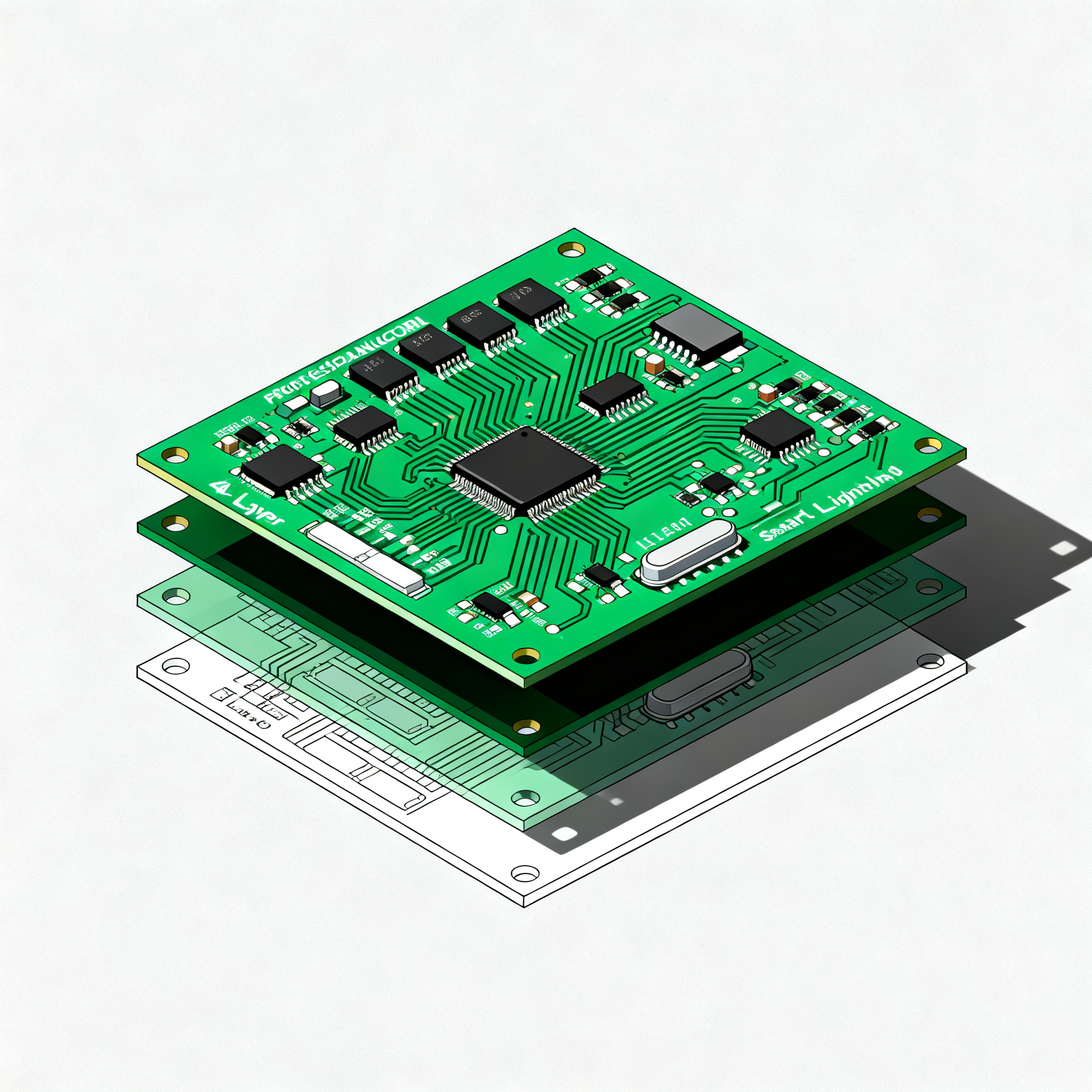
The Anatomy of a 4-Layer Smart Lighting Control PCB: Stackup, Materials, and Wireless Integration
A modern smart lighting control module typically integrates a Bluetooth Low Energy (BLE) or Wi-Fi SoC, an LED driver IC capable of PWM dimming, a microcontroller for logic and sensor fusion, and power management circuitry—all on a single board. The 4-layer PCB provides the necessary routing density and signal integrity without the cost and complexity of higher layer counts. The de facto stackup for wireless lighting controllers is:
- Layer 1 (Top): Critical signals, RF antenna traces, and components
- Layer 2 (Inner 1): Solid ground plane
- Layer 3 (Inner 2): Power plane (possibly split for analog/digital domains)
- Layer 4 (Bottom): Additional signals, low-speed routing, and thermal pads
This arrangement places the ground plane directly beneath the top layer, creating a controlled impedance environment for antenna traces and high-speed digital lines. The power plane on layer 3 provides low-inductance distribution to LED drivers that may demand several amps during PWM peaks. For thermal stability, high-Tg FR4 (glass transition temperature ≥ 170°C) is the baseline material; standard FR4 with a Tg of 130–140°C can soften during reflow or sustained high-power operation, leading to delamination and field failures.
The table below summarizes key FR4 material properties that directly impact smart lighting PCB performance, drawn from the ApolloPCB FR4 material specification sheet.
| Parameter | Standard FR4 | High-Tg FR4 | Unit/Notes |
|---|---|---|---|
| Glass Transition Temperature (Tg) | 130–140 | 170–180 | °C; higher Tg resists warpage during lead-free reflow |
| CTE (Z-axis, below Tg) | 50–70 | 45–55 | ppm/°C; lower CTE reduces via barrel stress |
| Dielectric Constant (Dk) @ 1 MHz | 4.2–4.8 | 4.0–4.6 | Lower Dk benefits RF signal speed |
| Dissipation Factor (Df) @ 1 MHz | 0.015–0.025 | 0.012–0.020 | Lower Df reduces signal loss |
| Thermal Conductivity | 0.3–0.4 | 0.3–0.4 | W/m·K; FR4 is a poor thermal conductor—thermal vias essential |
| Moisture Absorption | 0.1–0.2% | 0.1–0.15% | Lower moisture uptake improves CAF resistance |
| Flammability Rating | V-0 | V-0 | UL 94; mandatory for enclosed luminaires |
While FR4 handles the control and RF circuitry, the LED driver section often demands careful thermal design. High-power LEDs themselves are frequently mounted on metal-core PCBs (MCPCBs), but the driver IC and MOSFETs on the 4-layer FR4 board still dissipate significant heat. Designers use thermal vias under exposed pads, 2 oz copper on power layers, and sometimes a hybrid approach that bonds an aluminum substrate to the FR4 stack. The ApolloPCB SMD LED package size guide provides footprint recommendations for common packages like 2835, 5050, and 5630, ensuring that the LED solder pads can handle the current density without excessive voltage drop.
Wireless integration adds another layer of complexity. A BLE module like the Nordic nRF52 series or an ESP32-based Wi-Fi/BLE combo requires a 50 Ω impedance-controlled antenna trace, a generous keep-out zone free of copper pours, and ground stitching vias along the board edge to suppress edge radiation. Placing the antenna far from the LED driver’s switching node—often the primary source of conducted and radiated EMI—is non-negotiable.
2-Layer vs. 4-Layer vs. Metal-Core: Choosing the Right PCB Architecture for Smart Lighting
Not every smart lighting product demands a 4-layer board. Cost-sensitive bulbs and simple on/off controllers may function adequately on two layers, while high-lumen fixtures with dense LED arrays often rely on metal-core PCBs for heat spreading. The decision hinges on signal integrity, thermal management, and manufacturing budget. The QueenEMS 2-layer vs. 4-layer decision guide clarifies that a 2-layer board routes all signals, power, and ground on just the top and bottom copper layers, whereas a 4-layer PCB adds two internal planes dedicated to VCC and GND—a game-changer for noise-sensitive wireless circuits.
Metal-core PCBs, as detailed by JHYPCB’s LED PCB types overview, excel at conducting heat away from LEDs but are typically single-layer for the thermal substrate. For smart lighting, a hybrid design often emerges: an FR4 4-layer board for the control and wireless logic, connected via board-to-board connectors or flex to an aluminum MCPCB that hosts the LED array. WonderfulPCB’s smart lighting control module guide emphasizes that the PCB is the main part of the module, and good design ensures longevity. The table below compares the three architectures against the key requirements of a wireless lighting controller.
| Comparison Metric | 2-Layer FR4 | 4-Layer FR4 | Metal-Core (Aluminum/Copper) | Selection Criteria & Failure Boundary |
|---|---|---|---|---|
| Signal Integrity / EMI | Poor; no dedicated ground plane, large loop areas | Excellent; solid ground plane adjacent to signal layer | Not applicable for complex digital/RF; typically single-layer | Choose 4-layer if BLE/Wi-Fi range and regulatory EMC are critical |
| Thermal Management (Driver IC) | Limited; relies on copper pours and thermal vias | Good; internal power plane helps spread heat, thermal vias to bottom | Excellent for LED heat; driver IC still needs FR4 area | Hybrid FR4+MCPCB if LED array >10W; otherwise 4-layer with heavy copper |
| Routing Density | Low; all signals on two layers, prone to crosstalk | High; two signal layers plus planes, controlled impedance possible | Very low; single-layer routing limits complexity | 4-layer mandatory for MCU + wireless + PWM driver in compact form factor |
| Cost (Prototype, 100×100mm) | $2–5 per board | $8–15 per board | $5–10 per board (single-layer) | 2-layer may suffice for non-wireless, low-power designs; 4-layer cost justified by reliability |
| Lead Time (Standard) | 3–5 days | 5–8 days | 5–7 days | 4-layer adds one lamination cycle; ENIG finish may extend by 1 day |
| Typical Application | Basic LED bulb, non-connected dimmer | BLE mesh lighting, Wi-Fi smart switch, sensor-integrated luminaire | High-bay LED panel, streetlight LED engine | Hybrid: 4-layer FR4 control board + MCPCB LED board for optimal performance |
AdvancedPCB’s 4-layer cost factors note that heavier copper (2 oz) and ENIG finish increase cost but are often necessary for current capacity and assembly yield. Panel efficiency also matters: a well-designed array with fiducials can reduce per-unit cost even at prototype volumes. For smart lighting, the 4-layer FR4 board is the backbone of the control system, while the MCPCB handles the photons. This separation of concerns allows each substrate to be optimized without compromise.
Designing for Manufacturability: Layout Pitfalls, Component Selection, and Assembly Tips for Wireless Lighting Boards
A flawless schematic means nothing if the layout invites EMI, thermal runaway, or assembly defects. The following guidelines, drawn from field experience and industry resources, target the most common failure modes in wireless lighting control PCBs.
Antenna Keep-Out Zones and Ground Stitching. For any on-board antenna (chip, PCB trace, or module), define a copper-free area on all layers that extends at least 5 mm beyond the antenna footprint. The ground plane on layer 2 should be continuous under the RF section, and the board edge should be lined with closely spaced stitching vias (≤ λ/20 spacing) to suppress fringing fields. Place the wireless module as far as practical from the LED driver’s switching inductor and MOSFETs—at least 15 mm separation, with the ground plane acting as a shield.
Thermal Relief for LED Drivers. High-current LED drivers like the Texas Instruments TPS92515 or Onsemi NCL30160 can dissipate several watts. Use a solid copper area on the bottom layer under the driver IC, connected by a dense array of thermal vias (0.3 mm hole, 0.6 mm pad, plated shut if possible). Avoid thermal relief spokes on these vias; direct connection to the copper pour maximizes heat transfer. For boards with 2 oz inner copper, the power plane on layer 3 can double as a heat spreader.
BOM Optimization to Avoid Shortages. The Accuristech study found that 68% of teams have messy BOM data, and 60% are surprised by component shortages. For smart lighting, the wireless SoC and LED driver are often single-sourced. Mitigate risk by pre-qualifying pin-compatible alternatives (e.g., ESP32-C3 vs. ESP32-S3, or a drop-in BLE module from a different vendor) and locking them into the BOM as approved alternates. Avoid post-freeze changes: 51% of teams make them, and each change can cost $50,000 or more in rework and delayed NPI.
Surface Finish and Assembly Yield. ENIG (Electroless Nickel Immersion Gold) is the preferred finish for smart lighting boards with fine-pitch QFN packages, BGA wireless modules, and dense SMD LEDs. Its flatness ensures coplanarity, and the gold layer prevents oxidation during storage. HASL (Hot Air Solder Leveling) may be acceptable for through-hole connectors on cost-constrained designs, but the uneven surface can cause opens on 0.5 mm pitch components. The HCDPCBA LED PCB assembly guide highlights that Automated Optical Inspection (AOI) and flying probe testing are essential for catching solder defects and shorts on dense LED driver boards. AOI can detect missing components, tombstoning, and insufficient solder on LED pads, while flying probe verifies net connectivity and passive component values.
The table below summarizes critical DFM parameters that directly affect assembly yield and long-term reliability for 4-layer wireless lighting boards.
| DFM Parameter | Recommended Value | Rationale / Failure Mode Avoided |
|---|---|---|
| Minimum Trace/Space (outer layers) | 5/5 mil (0.127/0.127 mm) | Prevents shorts and etching defects; supports 50 Ω RF traces |
| Minimum Drill Size | 0.3 mm (12 mil) | Standard for low-cost fabrication; smaller vias increase cost |
| Via Aspect Ratio | ≤ 8:1 | Ensures reliable plating; higher ratios risk barrel cracks under thermal cycling |
| Copper Weight (inner layers) | 1 oz (35 µm), 2 oz for power plane | 2 oz on layer 3 reduces IR drop for LED driver current pulses |
| Surface Finish | ENIG (3–5 µm Ni, 0.05–0.1 µm Au) | Flatness for QFN/BGA; prevents oxidation; compatible with RF |
| Solder Mask Clearance | 2 mil (0.05 mm) expansion | Avoids mask registration errors on fine-pitch LED pads |
| Fiducial Marks | 3 global fiducials, 1 local per fine-pitch IC | Enables accurate pick-and-place; reduces tombstoning on 0402 LEDs |
| Test Point Access | ≥ 1.0 mm diameter pads on bottom | Flying probe access for net verification; avoids bed-of-nails cost |
Engage your PCB manufacturer early—ideally during schematic capture. Share the proposed stackup, impedance requirements, and critical component placements. A quick design review can catch antenna keep-out violations, insufficient thermal relief, or BOM risks before they become locked into the layout. The AllPCB field failure analysis framework emphasizes that most field returns trace back to overlooked DFM rules, not component defects. Building in reliability from the start is far cheaper than a recall.
Smart Lighting Control PCB Assembly: Questions Engineers and Buyers Ask Before Prototyping
Q: What 4-layer stackup do you recommend for a wireless smart lighting controller with BLE and high-current LED drivers?
A: The standard stackup is Signal (top) – GND – PWR – Signal (bottom). The solid ground plane on layer 2 provides a low-impedance return path and controlled impedance for the antenna trace (typically 50 Ω). If your design includes sensitive analog sensors alongside digital PWM, split the power plane on layer 3 into analog and digital sections, connected at a single point near the power supply input. This prevents digital noise from coupling into analog front-ends. For high-current LED drivers, use 2 oz copper on the power plane and stitch thermal vias from the driver’s exposed pad to the bottom copper pour.
Q: How do I prevent wireless interference from LED PWM dimming on the same board?
A: PWM dimming at frequencies between 200 Hz and 2 kHz generates harmonics that can desensitize a BLE receiver. Mitigation steps: (1) Define a generous antenna keep-out zone—at least 5 mm on all layers, with no copper pours or traces. (2) Place the wireless module and antenna on the opposite side of the board from the LED driver and its switching inductor. (3) Use ground stitching vias along the board edge near the RF section to contain edge radiation. (4) Consider spread-spectrum clocking on the LED driver if the IC supports it; this smears the EMI energy across a wider band, reducing peak noise. (5) Add a series ferrite bead and shunt capacitor on the LED driver’s power input to attenuate conducted emissions.
Q: What are the typical minimum order quantities (MOQs) for prototype assembly of 4-layer smart lighting PCBs?
A: Most PCBA shops accept prototype orders as low as 5–10 boards. However, the per-unit cost drops significantly at 50+ units because panel utilization improves and setup charges are amortized. For 4-layer boards with ENIG finish, expect a minimum panel charge that may cover up to 10–15 small boards. If your design includes blind or buried vias, MOQs may rise to 25–50 pieces due to sequential lamination costs. Always request a quote for both 10-piece and 100-piece quantities to understand the cost inflection point.
Q: Should I specify ENIG or HASL surface finish for a smart lighting control board?
A: ENIG is strongly preferred for any board with fine-pitch components (0.5 mm pitch QFN, BGA wireless modules) or high-density SMD LEDs. Its flat surface ensures consistent solder paste printing and reduces the risk of opens or shorts. ENIG also resists oxidation during storage, which is critical for wireless modules that may sit in inventory before assembly. HASL (lead-free) can work for through-hole connectors and larger components if cost is the primary driver, but the uneven surface can cause coplanarity issues on LED pads, leading to tombstoning. For smart lighting, the marginal cost increase of ENIG (typically $0.50–$2 per board) is a worthwhile investment in assembly yield.
Q: How do I qualify a PCBA supplier for smart lighting modules to avoid field failures like the Ford recall?
A: Look for a supplier with IPC-A-610 Class 2 or Class 3 certification, which ensures workmanship standards for electronic assemblies. Verify that they have in-house AOI and flying probe testing—these catch solder defects and netlist errors before boards ship. Ask about their RF design experience: have they built BLE or Wi-Fi lighting products before? Request a documented failure analysis process, including cross-sectioning, X-ray, and thermal imaging capabilities. Finally, ask for references from similar IoT lighting projects and check their track record for on-time delivery and post-delivery support. A supplier that proactively suggests DFM improvements during the design review is a partner, not just a vendor.
At NovaPCBA, we specialize in 4-layer smart lighting control PCB assembly, offering ENIG finish, automated optical inspection, and rapid prototyping from 5 pieces. Our engineering team reviews every design for antenna keep-out compliance, thermal management, and BOM risk before fabrication begins. Contact us to discuss your next wireless lighting project and ensure your boards are built to avoid the field failures that made headlines.
References & Further Reading
- Ford Mustang Mach-E Recalled Over Failing Exterior Lighting – Ford Authority
- NHTSA Recall 25V885 – Light Driver Control Module B (LDCMB)
- The Hidden Cost of Redesigning PCBs Around Missing Electronic Components – Accuristech
- From Failure to Fix: A Practical Guide to PCBA Field Failure Analysis – AllPCB
- 2 Layer vs 4 Layer PCB: 2-Minute Decision Guide – QueenEMS
- 6 Types of LED PCB Boards: Aluminum vs Copper vs FR4 vs Ceramic – JHYPCB
- Understanding 4 Layer PCB: Key Benefits for Engineers – AdvancedPCB
- Smart Lighting Control Module Design and Manufacturing – WonderfulPCB
- FR4 PCB Material Specification Sheet – ApolloPCB
- LED PCB Assembly: Lighting Control PCB Manufacturing – HCDPCBA
- SMD LED Package Size Chart & LED PCB Assembly Guide – ApolloPCB