Selecting the Right Equipment for PCB Assembly: A Comparative Guide for Efficiency and Cost-Effectiveness
Introduction In the fast-paced world of electronics, selecting the right equipment for PCB assembly is crucial for ensuring efficiency and cost-effectiveness. With the increasing complexity of electro...
Introduction
In the fast-paced world of electronics, selecting the right equipment for PCB assembly is crucial for ensuring efficiency and cost-effectiveness. With the increasing complexity of electronic devices, the demand for precise and reliable PCB assembly has never been higher. Understanding how to choose the right components and equipment not only impacts the functionality and performance of the final product but also affects production costs and time-to-market. This article provides a comprehensive guide to selecting the right equipment for PCB assembly, focusing on component specifications, datasheets, selection criteria, and application circuits.
Technical Overview
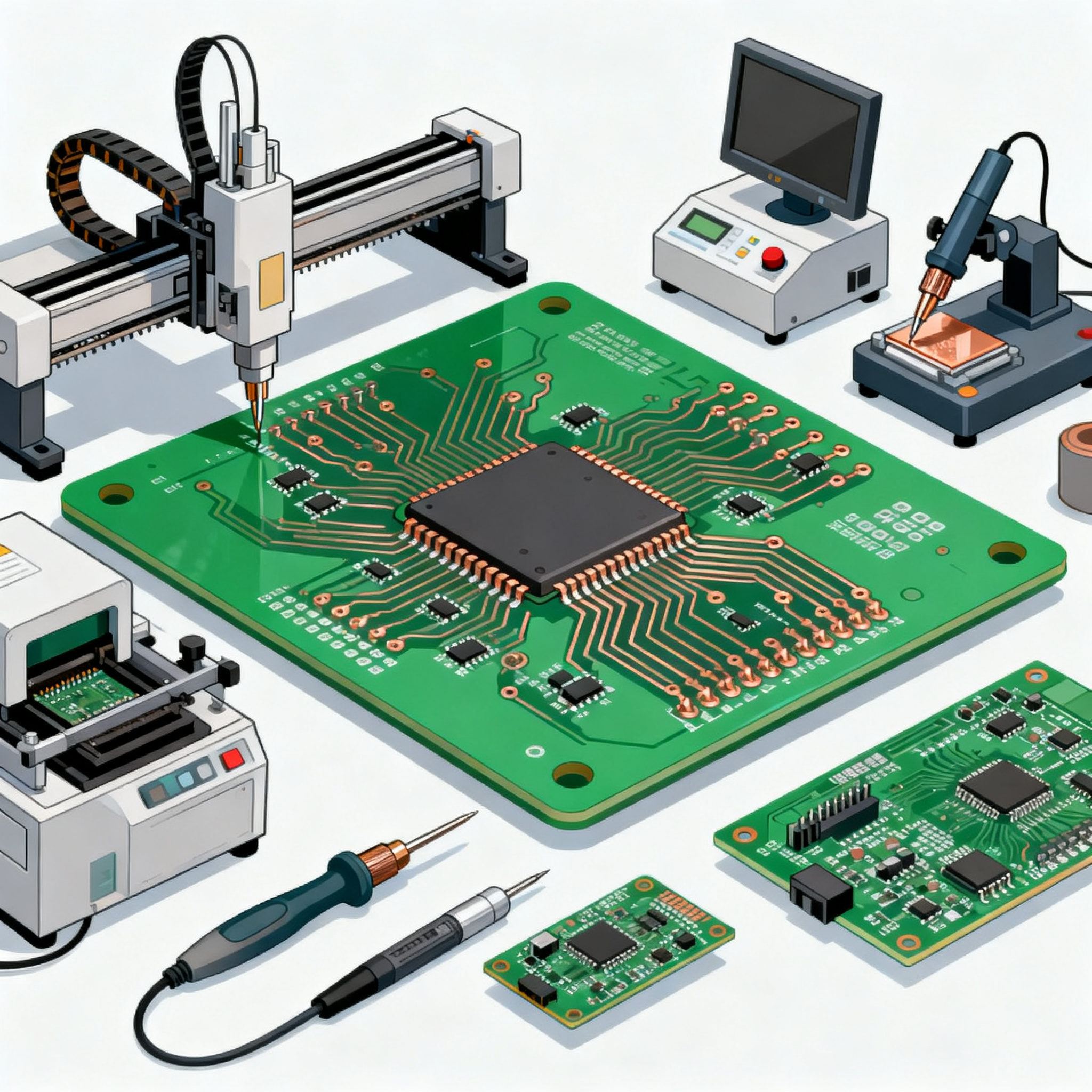
The architecture of PCB assembly involves several critical components and processes. At its core, PCB assembly transforms a bare board into a sophisticated electronic device by mounting components onto it. The main stages include solder paste application, pick and place of components, soldering, inspection, and testing. Each stage requires specific equipment, such as solder paste printers, pick and place machines, reflow ovens, and automated optical inspection (AOI) systems.
Understanding the principles of each stage is essential for selecting the right equipment. For instance, the accuracy of a pick and place machine significantly impacts the assembly's overall quality, while the precision of a solder paste printer affects the solder joint integrity. Therefore, a thorough understanding of these core concepts is vital for making informed equipment choices.
Detailed Specifications
When selecting components for PCB assembly, core specifications play a pivotal role. Key specifications include CPU speed, memory capacity, available peripherals, power requirements, and package type. These factors determine the component's performance and compatibility with the overall system. Below is a table summarizing the core specifications of typical components used in PCB assembly.
| Specification | Component A | Component B |
|---|---|---|
| CPU Speed | 2.4 GHz | 1.8 GHz |
| Memory | 4 GB | 2 GB |
| Peripherals | USB, HDMI | USB, Ethernet |
| Power | 5V, 2A | 3.3V, 1.5A |
| Package | BGA | QFP |
| Temperature Range | -40°C to 85°C | -20°C to 70°C |
| Clock Speed | 500 MHz | 400 MHz |
| Data Rate | 10 Gbps | 5 Gbps |
| Dimensions | 15x15 mm | 12x12 mm |
| Operating Voltage | 1.2V | 1.8V |
Key Takeaways from the Specifications
The core specifications table highlights the differences between two components, allowing engineers to make informed decisions based on performance requirements and constraints. For instance, Component A offers higher CPU speed and memory, making it suitable for applications requiring high processing power and data handling. On the other hand, Component B, with lower power requirements and smaller dimensions, might be more suitable for compact, energy-efficient designs. Understanding these specifications helps in aligning the component choice with the intended application and overall system design.
Electrical Characteristics
Electrical characteristics are critical in determining a component's compatibility and performance within a PCB assembly. Key parameters include voltage, current, timing, and I/O specifications. These characteristics ensure that the component can operate effectively within the specified electrical environment. The following table provides a detailed comparison of the electrical characteristics of different components.
| Characteristic | Component A | Component B |
|---|---|---|
| Operating Voltage | 1.2V - 3.3V | 1.8V - 5V |
| Current Consumption | 150 mA | 200 mA |
| Input/Output Voltage | 0.8V - 1.8V | 0.9V - 2.5V |
| Timing (ns) | 10 ns | 15 ns |
| I/O Ports | 16 | 12 |
| Power Dissipation | 500 mW | 750 mW |
| Impedance | 50 Ohms | 75 Ohms |
| Frequency Range | DC to 2 GHz | DC to 1.5 GHz |
| Leakage Current | 5 µA | 10 µA |
| ESD Protection | ±15 kV | ±10 kV |
| Thermal Resistance | 50°C/W | 60°C/W |
Practical Implications
The table of electrical characteristics provides insights into how each component will perform under different electrical conditions. Component A, with its wider operating voltage range and lower power dissipation, is ideal for applications where energy efficiency is critical. In contrast, Component B might be preferred in applications requiring robust ESD protection. These characteristics help engineers ensure that the selected components can reliably function within the system's electrical parameters, minimizing the risk of malfunction or damage.
Application Comparison
Different components serve various applications, and understanding their use cases is essential for effective selection. The table below compares different configurations and applications where these components can be utilized.
| Application | Component A | Component B |
|---|---|---|
| Embedded Systems | High performance | Cost-effective |
| Consumer Electronics | Advanced features | Basic functionality |
| Automotive | Temperature resistant | Standard use |
| Industrial Automation | Reliable and durable | Moderate usage |
| IoT Devices | Low power | Compact size |
| Telecommunications | High data rate | Standard data rate |
| Medical Devices | Precision control | General monitoring |
| Networking Equipment | High throughput | Basic connectivity |
Application Guidelines
The application comparison table highlights how different components are best suited for specific use cases. Component A is tailored for high-performance applications such as embedded systems and telecommunications, where advanced features and high data rates are essential. Conversely, Component B is ideal for cost-sensitive applications like consumer electronics and IoT devices, where compact size and basic functionality are prioritized. Understanding these applications helps engineers choose components that align with the project's objectives and constraints.
Design Considerations
Designing a PCB assembly involves several critical considerations to ensure optimal performance and reliability. Engineers must evaluate the thermal management techniques to dissipate heat effectively, select appropriate materials to match the environmental conditions, and ensure signal integrity by minimizing electromagnetic interference (EMI). Additionally, understanding the assembly process's constraints, such as component placement accuracy and solder joint quality, is crucial. Compliance with industry standards, such as IPC-A-610 for assembly and IPC-2221 for design, is also essential to maintain quality and reliability. By carefully considering these factors, engineers can design efficient and cost-effective PCB assemblies that meet the required specifications and performance criteria.
Step-by-Step Implementation
- Define the project requirements, including performance, cost, and size constraints.
- Select appropriate components based on the detailed specifications and application guidelines provided in the tables.
- Design the PCB layout, ensuring compliance with IPC standards and considering thermal management and signal integrity.
- Procure the necessary equipment and components from reliable sources, ensuring compatibility with the assembly process.
- Assemble the PCB using the selected equipment, following best practices for solder paste application, component placement, and reflow soldering.
- Inspect the assembled PCB using AOI systems to identify any defects or inconsistencies.
- Perform functional testing to verify the PCB assembly's performance and ensure it meets the project requirements.
- Document the assembly process and test results for future reference and quality assurance.
Common Issues & Solutions
- Issue: Solder bridges causing short circuits. Solution: Adjust the solder paste stencil design and ensure proper alignment during application.
- Issue: Components not aligning correctly. Solution: Calibrate the pick and place machine for precise placement accuracy.
- Issue: Insufficient thermal management leading to overheating. Solution: Incorporate heat sinks and thermal vias to improve heat dissipation.
- Issue: PCB warping during reflow soldering. Solution: Use appropriate materials and design techniques to reduce thermal stress.
- Issue: Signal integrity issues due to EMI. Solution: Implement proper grounding and shielding techniques to minimize interference.
- Issue: Inconsistent solder joint quality. Solution: Optimize the reflow oven profile and ensure uniform heating across the PCB.
Applications & Use Cases
PCBs are integral to a wide range of applications, from consumer electronics and automotive systems to industrial automation and medical devices. In consumer electronics, PCBs enable compact and efficient designs for smartphones, tablets, and laptops. In the automotive industry, PCBs are used in engine control units, infotainment systems, and advanced driver-assistance systems (ADAS). Industrial automation relies on PCBs for controlling machinery and processes, while medical devices use PCBs for monitoring and diagnostic equipment. Understanding these applications helps engineers tailor their PCB designs to meet specific industry requirements.
Selection & Sourcing Guide
When selecting components for PCB assembly, sourcing from reliable suppliers is crucial to ensure quality and availability. IC Online offers a comprehensive selection of electronic components, providing detailed datasheets and specifications to assist in the selection process. By leveraging such resources, engineers can make informed decisions and ensure timely procurement of the necessary components for their projects.
FAQ
- What are the key factors to consider when selecting PCB assembly equipment? Consider factors such as precision, speed, compatibility with components, and cost-effectiveness.
- How do I ensure the quality of a PCB assembly? Follow industry standards, use reliable equipment, and perform thorough inspections and testing.
- What is the importance of component specifications in PCB design? Specifications determine compatibility, performance, and reliability within the system.
- How can I minimize EMI in my PCB design? Implement proper grounding, shielding, and trace routing techniques.
- What are the common causes of solder joint defects? Common causes include improper solder paste application, misaligned components, and incorrect reflow profiles.
- How can I improve thermal management in my PCB assembly? Use heat sinks, thermal vias, and appropriate material selection to enhance heat dissipation.
- What are the benefits of using automated optical inspection (AOI) systems? AOI systems provide fast and accurate defect detection, improving assembly quality and reducing rework.
- How do I choose between different package types for components? Consider factors such as size, thermal performance, and ease of assembly when selecting package types.
- What role does IPC compliance play in PCB design and assembly? IPC compliance ensures adherence to industry standards, improving quality, reliability, and interoperability.
- How can I reduce the cost of PCB assembly? Optimize the design for manufacturability, select cost-effective components, and negotiate with suppliers for better pricing.
Conclusion
Selecting the right equipment and components for PCB assembly is a critical aspect of electronics design and manufacturing. By understanding the core specifications, electrical characteristics, and application guidelines, engineers can make informed decisions that enhance efficiency and cost-effectiveness. Adhering to industry standards and leveraging reliable resources ensures high-quality PCB assemblies that meet the demands of various applications. This comprehensive guide provides the necessary insights and tools to navigate the complexities of PCB assembly, ultimately leading to successful project outcomes.