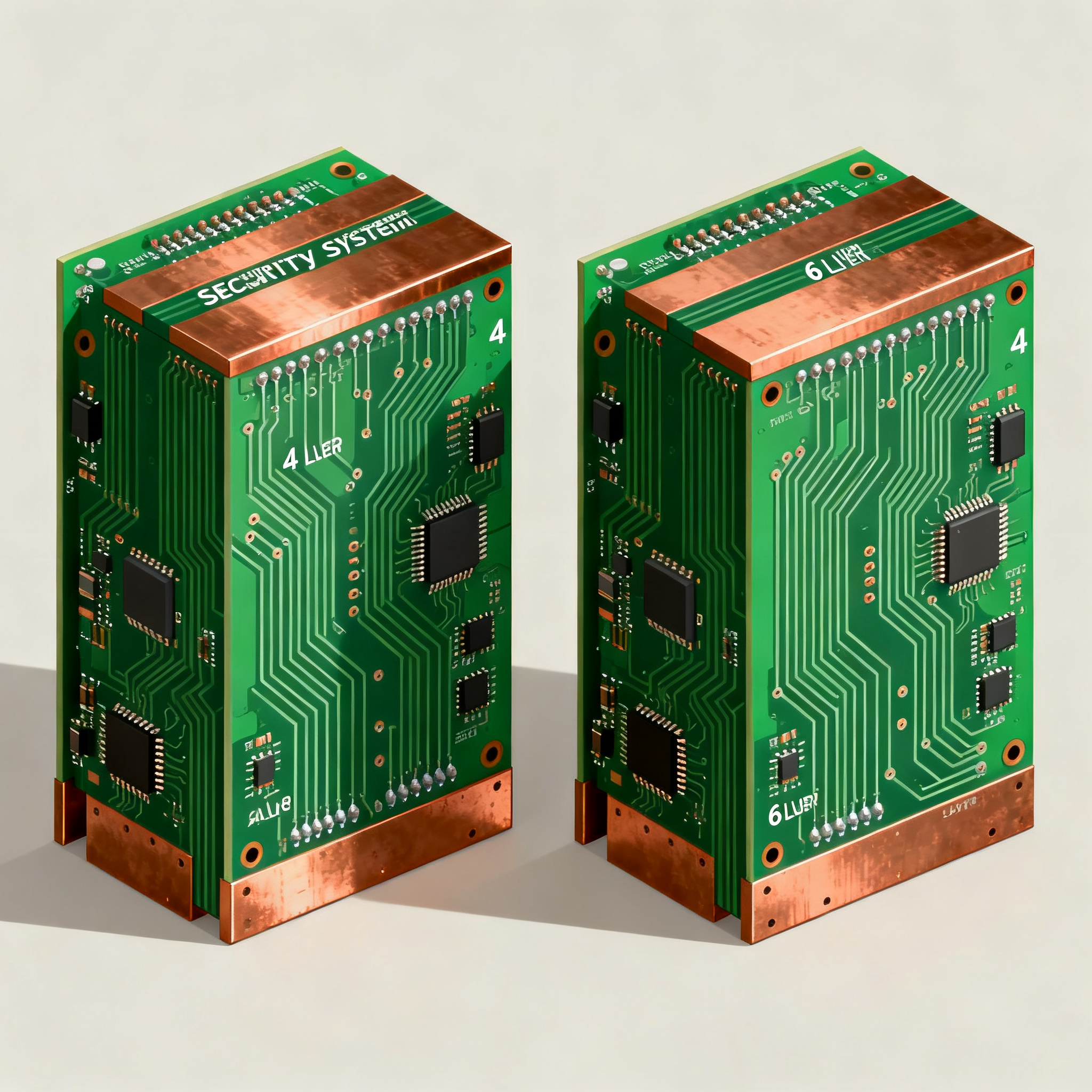
Security System PCB Assembly: 4-Layer vs. 6-Layer Thick Copper – A Side-by-Side Comparison for Design Engineers
Security System PCB Assembly: 4-Layer vs. 6-Layer Thick Copper — A Side-by-Side Comparison for Design Engineers Why Security System PCB Reliability Is Under Pressure Right Now Security system designer...
Security System PCB Assembly: 4-Layer vs. 6-Layer Thick Copper — A Side-by-Side Comparison for Design Engineers
Why Security System PCB Reliability Is Under Pressure Right Now
Security system designers are caught between two tightening constraints. On the supply side, the copper foil and FR‑4 laminate pipeline is under strain as AI server demand absorbs HTE and RTF copper foils, production equipment, and fabrication capacity that would normally serve industrial PCB volumes (Large Battery). On the field side, a single interconnect defect or short circuit can disable an alarm panel, PoE camera, or access controller—failures that trigger expensive truck rolls, false alarm fines, and even product recalls (Micrologix).
Thick-copper layers (≥2 oz) are essential for the high‑current paths that drive IR illuminators, magnetic locks, and backup battery chargers, but they magnify the risk of electrical shorts. Tight trace spacing, residual unetched copper, and foreign metal debris create unintended bridges between adjacent conductors, and these faults become more probable when copper thickness increases (FinestPCB). The stack-up decision—4‑layer versus 6‑layer—directly controls how you separate high‑current power from sensitive analog and high‑speed digital signals, and it determines whether your board can survive the drilling and plating stresses that thick copper introduces.
With lead times stretching and material premiums rising, you can’t afford to over‑engineer the layer count, but you also can’t afford field failures that stem from a compromised stack-up. The following sections give you a side‑by‑side technical and cost reality check, grounded in what security hardware actually needs.
What 4-Layer and 6-Layer Thick-Copper Stack-ups Actually Do for Security Devices
A standard 4‑layer PCB at 1.6 mm thickness delivers dedicated power and ground planes that significantly reduce EMI and provide clean signal return paths (PrototypeGuru; BestPCBs; PCBSync). For many access control panels and simple alarm communicators, this is enough: you route low‑speed digital on the outer layers, bury a solid ground plane on layer 2, and use layer 3 for a power plane that can carry 2–3 oz copper for solenoid and battery charging currents.
When you move to a 6‑layer stack, you gain two additional inner routing layers. This becomes critical for mixed‑signal security hardware that combines high‑speed video interfaces (MIPI, LVDS, SerDes), sensitive analog sensor front‑ends for PIR or microwave detectors, and PoE power management on a single board (Aivon). The extra layers let you partition ground planes—one solid reference for analog, one for digital—without splitting the power plane, and they give you room to route impedance‑controlled differential pairs away from high‑current switching nodes.
Thick copper (≥2 oz) on inner layers is often mandatory for security devices that must deliver 1–3 A continuous to IR LED arrays or door strikes. However, heavy copper introduces inner‑layer separation (ICD) risk. ICD occurs when the copper barrel inside a plated through‑hole separates from the inner‑layer copper pad, breaking the connection. This defect is driven by thermal stress and poor hole‑wall quality, and it becomes more likely when drilling through thick copper with small diameters (MCL PCB). Understanding the interplay of layer count, copper weight, and aspect ratio is the foundation of a reliable security PCB.
Key Stack-Up Parameters for Thick-Copper Security PCBs
| Parameter | 4‑Layer Thick Copper (Typical) | 6‑Layer Thick Copper (Typical) | Notes for Security Devices |
|---|---|---|---|
| Total board thickness | 1.6 mm (standard) | 1.6 mm or 2.0 mm | 1.6 mm fits standard connectors and enclosures; 2.0 mm adds rigidity for large panels. |
| Inner-layer copper weight | 2 oz (70 µm) on power/ground planes | 2 oz on dedicated power layers; 1 oz on signal layers | 2 oz supports 3–5 A continuous; above 2 oz raises ICD risk sharply. |
| Outer-layer copper weight | 1–2 oz finished | 1–2 oz finished | Heavy outer copper helps with thermal dissipation for LED drivers but complicates fine‑pitch soldering. |
| Typical via aspect ratio | 8:1 (0.2 mm hole in 1.6 mm) | 6:1 to 8:1 (0.3 mm hole in 2.0 mm) | Stay ≤8:1 to ensure reliable plating with thick copper; smaller holes risk ICD. |
| Impedance control capability | Limited to one or two differential pairs on outer layers | Multiple inner‑layer pairs with solid reference planes | Essential for 4K MIPI/LVDS cameras; 6‑layer avoids split‑plane discontinuities. |
| Typical dielectric spacing | 0.2–0.3 mm core/prepreg | 0.1–0.2 mm for high‑speed layers | Thinner dielectrics improve crosstalk isolation but raise cost. |
| Thermal conductivity (FR‑4) | ~0.3 W/m·K | ~0.3 W/m·K | Heavy copper planes act as heat spreaders; consider metal‑core IMS for extreme IR arrays. |
| Surface finish compatibility | OSP or ENIG | ENIG preferred for fine‑pitch BGAs | HASL not recommended on thick copper due to uneven pad surfaces. |
The table above highlights why a 6‑layer board isn’t just “more layers.” It’s a different design envelope: you can run 2 oz copper on dedicated power planes while keeping signal layers at 1 oz, preserving fine‑line etching and impedance control. In a 4‑layer design, forcing 2 oz copper onto a shared power/ground plane often means sacrificing signal integrity because the thicker copper widens trace geometries and reduces the space available for controlled impedance routing.
4-Layer vs. 6-Layer Thick Copper: A Stack-Up and Cost Reality Check
The cost delta between a 4‑layer and 6‑layer thick-copper board is not linear. A 6‑layer PCB typically costs about 65% more than an equivalent 4‑layer design when all other variables are held constant (AtlasPCB). The extra expense comes from additional lamination cycles, longer drill times for deeper vias, and tighter aspect ratio requirements that demand slower feed rates and more frequent bit changes (GREATPCB). However, this premium can be offset—or even reversed—when a 6‑layer stack eliminates the need for exotic laminates, blind vias, or split‑plane workarounds that a 4‑layer board would otherwise require.
Consider a PoE security camera that must route four lanes of MIPI at 2.5 Gbps alongside a 2 A IR LED driver. On a 4‑layer board, you might be forced to split the ground plane to isolate the noisy LED return path, creating a discontinuity in the video signal’s return current. To recover signal integrity, you might then need a low‑loss laminate like Megtron 6, which can push the board cost beyond that of a standard FR‑4 6‑layer stack. In such cases, the 6‑layer board on standard FR‑4 can deliver equivalent or better signal performance at a lower total cost than a heavily compromised 4‑layer design (Wonderful PCB).
Surface finish selection further influences cost and assembly yield. ENIG (Electroless Nickel Immersion Gold) adds $10–25 per panel but provides the flat pad surface necessary for fine‑pitch BGAs and QFNs found on image processors and AI accelerators. OSP (Organic Solderability Preservative) is cheaper and works well with thick copper, but it’s less forgiving for multiple reflow cycles. HASL is generally avoided on thick-copper security boards because the uneven pad topography can cause soldering defects on heavy copper pads (AtlasPCB). Via technology also matters: through‑hole vias keep lamination to a single cycle and avoid the cost and registration challenges of blind/buried vias, which is why most security system designs stick with through‑holes unless density forces otherwise (AdvancedPCB).
Side-by-Side Comparison: 4‑Layer vs. 6‑Layer Thick Copper for Security Systems
| Comparison Metric | 4‑Layer Thick Copper (2 oz Inner) | 6‑Layer Thick Copper (2 oz Power, 1 oz Signal) | Selection Criteria & Failure Boundary |
|---|---|---|---|
| Per‑unit cost (10k volume) | Baseline (e.g., $4.50–$6.00) | ~65% higher ($7.50–$10.00) | Use 4‑layer when signal density is low; go 6‑layer if it avoids exotic laminates or blind vias. |
| Signal integrity for 4K video | Marginal; requires careful floorplanning and possibly split planes | Excellent; dedicated ground planes and controlled impedance layers | If MIPI/LVDS eye diagrams close at 4‑layer, 6‑layer is the safer path without laminate upgrades. |
| Thermal management (2 A IR LED) | Heavy copper planes spread heat, but limited routing space for thermal vias | Extra layers allow dedicated thermal via arrays and better heat distribution | For continuous 2 A+ LED strings, 6‑layer helps avoid hot spots that degrade FR‑4. |
| ICD risk with 0.3 mm vias | Moderate; 2 oz inner layers can be drilled with 0.3 mm at 8:1 aspect ratio | Higher if 2 oz layers are stacked; requires strict process control | Keep aspect ratio ≤8:1 and specify 2 oz max on inner layers to minimize ICD (MCL PCB). |
| EMI/EMC performance | Good with solid ground plane; susceptible to noise coupling from high‑current switching | Very good; separate analog and digital ground planes reduce crosstalk | Critical for multi‑sensor cameras that combine analog PIR and digital video. |
| Design cycle time | Faster; fewer layers to route | Longer; more complex stack-up and impedance calculations | If time‑to‑market is king, a well‑executed 4‑layer may win; but respins from SI issues cost more. |
The comparison makes it clear: 6‑layer thick copper is not an automatic upgrade. It’s a strategic choice that pays off when signal density, noise isolation, or thermal demands push a 4‑layer design beyond its practical limits. For many access control and basic alarm boards, a 4‑layer stack with 2 oz inner planes remains the cost‑effective workhorse.
Where Security Systems Really Use 4- and 6-Layer Thick Copper
Real security system footprints reveal a clear split. 4‑layer thick copper dominates in access control panels, where the primary electrical loads are solenoid drivers (12–24 V, 1–2 A pulse), battery charging circuits, and low‑speed RS‑485 or Wiegand communication. These boards typically need 2–3 oz copper on the power plane to handle surge currents without excessive voltage drop, but the signal density is low enough that two routing layers are sufficient. A 1.6 mm 4‑layer board with a solid ground plane and a thick power plane delivers the necessary current capacity and EMI control without over‑engineering.
6‑layer thick copper shines in multi‑sensor outdoor cameras and advanced alarm control units that combine high‑resolution video, audio, onboard analytics, and power‑over‑Ethernet. A typical design might include a 4K image sensor with MIPI output, a stereo audio codec, an IR‑LED driver delivering 2 A continuous, and a PoE PD controller that negotiates up to 25.5 W. The Aivon security components guide underscores how analog sensor front‑ends in intrusion detectors demand excellent noise isolation and low‑noise grounding to prevent false alarms. A 6‑layer stack lets you assign one inner layer as a dedicated analog ground, another as a digital ground, and still have room for a 2 oz power plane and controlled‑impedance video routing—all without resorting to blind vias.
Another growing application is AI‑enabled edge cameras that run object classification locally. These boards often carry a multi‑core processor with DDR memory and a BGA package, requiring fine‑pitch routing and ENIG finish. The 6‑layer thick-copper stack accommodates the high‑current LED drivers on one side and the dense digital routing on the other, with thermal vias stitching the power planes to a heatsink or metal enclosure. In these designs, the extra two layers are not a luxury; they are the difference between a board that passes EMC on the first spin and one that radiates noise into the analog sensor chain.
Application Matrix: Security System Type vs. Recommended Stack-Up
| Security System Type | Typical Loads & Signals | Recommended Stack-Up | Key Design Considerations |
|---|---|---|---|
| Access control panel (single door) | 12 V solenoid, Wiegand, RS‑485, battery charger | 4‑layer, 2 oz inner power plane | Keep power and signal returns separate; use 1.6 mm FR‑4. |
| Multi‑door networked controller | Multiple solenoids, Ethernet, PoE, tamper sensors | 4‑layer (if low video) or 6‑layer (if integrated camera) | Watch for ground bounce from simultaneous solenoid firing. |
| Outdoor PoE PTZ camera | 4K MIPI, IR LED 2 A, heater, audio, motor drivers | 6‑layer, 2 oz on dedicated power layers | Isolate motor PWM return from video ground; use ENIG for image sensor BGA. |
| Multi‑sensor fixed camera (360°) | Multiple MIPI streams, IR LEDs, onboard AI processor | 6‑layer, 1 oz signal, 2 oz power | High layer count may be needed; consider 8‑layer if DDR routing is dense. |
| Wireless alarm hub with touchscreen | LCD interface, Wi‑Fi/BLE, siren driver, battery backup | 4‑layer, 2 oz power plane | Keep RF section isolated; use 4‑layer with careful partitioning. |
| Edge AI camera (object classification) | 4K sensor, DDR4, NPU, PoE++, IR LED | 6‑layer thick copper (2 oz power) | ENIG mandatory; thermal vias under NPU; avoid blind vias if possible. |
This matrix isn’t rigid, but it reflects the inflection point where 6‑layer becomes the lower‑risk choice. If your design includes any combination of high‑resolution video, high‑current LED drive, and sensitive analog detection, a 6‑layer stack-up will almost certainly save you time and respins.
How to Choose the Right Stack-Up Without Over-Engineering Your BOM
Start with the power plane current requirement. If your board must deliver more than 2 A continuous on an inner layer, 2 oz copper is the practical maximum for reliable through‑hole plating on a 1.6 mm board with 0.3 mm vias. Verify with your fabricator that they can maintain a 0.3 mm finished hole through a 2.0 mm thick stack without inner‑layer separation; the ICD failure boundary tightens quickly above 2 oz (MCL PCB). If your current demands exceed what 2 oz can handle, consider widening traces and adding parallel planes before jumping to 3 oz, which often forces larger drill diameters and reduces routing density.
Standardize on 1.6 mm total thickness and FR‑4 laminate unless your high‑speed interfaces (e.g., 4K MIPI at 2.5 Gbps) demand a lower‑loss material. Using standard specifications keeps lead times short and avoids the premium associated with specialty laminates (Wonderful PCB). When you do need controlled impedance, work with your fabricator to define a stack-up that uses standard prepreg and core thicknesses—this avoids custom material charges.
Avoid blind and buried vias unless absolutely necessary for routing density. Through‑hole vias keep the lamination cycle count to one and significantly reduce cost, especially on thick-copper boards where laser drilling blind vias is challenging (AdvancedPCB). If you must escape a 0.5 mm pitch BGA, a 6‑layer board with through‑vias can often do the job if you plan the pinout carefully, whereas a 4‑layer board might force blind vias.
On surface finish, use OSP for boards that carry only coarse‑pitch components and no BGAs. It’s the most cost‑effective finish and works well with thick copper. Switch to ENIG only when you have fine‑pitch BGAs or QFNs that demand flat pads; the $10–25 per panel premium is justified by higher assembly yield and fewer field failures from opens (AtlasPCB). Never use HASL on thick-copper security PCBs—the uneven surface can cause tombstoning and solder bridging on heavy copper pads.
Finally, factor the 2026 copper foil shortage into your sourcing strategy. AI server demand is absorbing HTE and RTF copper foils, extending lead times for standard FR‑4 boards. Lock in multi‑source supply agreements early, and design with 1 oz copper on signal layers wherever possible to reduce your exposure to thick‑foil bottlenecks (Large Battery). Consolidating panel layouts and ordering larger quantities also helps stabilize pricing and secure capacity.
Tip: Before finalizing your stack-up, request a cross‑section coupon from your fabricator for the exact copper weights and via sizes you plan to use. This validates plating quality and ICD resistance before production, saving weeks of troubleshooting later.
Security System PCB Assembly: Stack-Up Questions Engineers and Buyers Ask
Q: When does a 6-layer PCB actually save money over a 4-layer board in a security system?
When routing dense mixed‑signal circuits—such as a PoE camera with 4K video, audio, and IR LED drivers—forces a 4‑layer board to add multiple split planes and increase copper thickness, the 6‑layer stack can eliminate the need for exotic laminates or blind vias. In many cases, a standard FR‑4 6‑layer board costs less than a heavily compromised 4‑layer design that requires Megtron 6 or similar low‑loss materials to meet signal integrity targets.
Q: What is the maximum copper weight I can use on inner layers without risking ICD?
Most fabricators limit inner‑layer copper to 2 oz (70 µm) for standard 1.6 mm 6‑layer boards with 0.3 mm through‑holes. Above 2 oz, the risk of inner‑layer separation during drilling rises sharply, requiring larger drill diameters and heavier process control (MCL PCB). If your design demands 3 oz, expect to use 0.4 mm minimum hole sizes and work closely with the fabricator on a qualified process.
Q: How does the 2026 copper foil shortage affect security system PCB assembly quotes?
The shortage, driven by AI server demand, is squeezing availability of HTE and RTF copper foils used in FR‑4 boards. Long lead times and price premiums are expected; securing multi‑source supply agreements and using standard 1 oz copper where possible helps mitigate delays (Large Battery). Some fabricators are offering allocation‑based pricing, so early commitment is key.
Q: Can I use a 4-layer thick-copper board for a multi‑sensor outdoor camera with IR LEDs and 4K video?
It’s possible with careful floorplanning, but you’ll likely need to isolate the high‑current IR LED return path on a dedicated layer and keep video signals on the opposite side. A 6‑layer board gives you an extra dedicated ground plane, reducing crosstalk and simplifying the layout without driving up cost drastically. If the camera also includes audio or radar, the 6‑layer stack is the safer bet.
Q: What surface finish is best for thick-copper security PCBs with fine-pitch components?
ENIG provides flat pads for fine‑pitch BGAs and QFNs common in image processors, but adds cost. For boards without fine‑pitch parts, OSP keeps costs low and is compatible with thick copper. HASL is not recommended because uneven pad surfaces can cause soldering issues on heavy copper pads (AtlasPCB).
Q: What aspect ratio should I target for vias in a 6‑layer thick-copper security board?
Aim for an aspect ratio of 8:1 or lower. For a 1.6 mm board, that means a minimum finished hole size of 0.2 mm. If you go to 2.0 mm thickness, use 0.3 mm drills to stay within the 6:1 to 8:1 range that most fabricators can reliably plate with thick copper (GREATPCB). Tighter ratios increase the risk of voids and ICD.
Choosing between a 4‑layer and 6‑layer thick-copper stack-up for security systems is a balancing act between current capacity, signal integrity, and cost. The right answer depends on the specific mix of loads and signals on your board. At NovaPCBA, we’ve assembled thousands of security system PCBs—from simple access controllers to multi‑sensor AI cameras—and our engineering team can help you validate your stack-up, select the right surface finish, and lock in supply during the copper shortage. When every layer counts, a partner who understands thick-copper processing and mixed‑signal security design makes the difference between a board that works on the bench and one that survives years in the field.
References & Further Reading
- PCB Defects: Complete Guide to Prevention, Root Causes, and High-Yield Assembly — FinestPCB
- Common PCB Defects: Causes, Solutions, and Prevention — Micrologix
- 2026 PCB Material Shortage: Impact on BMS Boards — Large Battery
- PCB Issue Guide: PCB Failure Analysis and Common Issues — MCL PCB
- 2-Layer vs 4-Layer vs 6-Layer PCB Cost Comparison — GREATPCB
- 6 Layers PCB Manufacturing: Advanced Stack-up, Design Guidelines, and Cost Analysis — Wonderful PCB
- Multilayer PCB Cost: Why 6-Layer Costs 65% More Than 4-Layer — AtlasPCB
- Improving Signal Integrity with 4 Layer PCB Technology — AdvancedPCB
- PCB Thickness Guide 2026 — PrototypeGuru
- Standard PCB Thickness Chart — EBest PCB
- PCB Thickness Guide: Standards, Selection Factors & Best Practices — PCBSync
- Security System Components and Their Functions — Aivon