Reducing PCB Production Lead Times: Proven Strategies for Faster Turnarounds
Introduction In the ever-evolving electronics industry, reducing PCB production lead times is crucial for staying competitive. As consumer demands grow and product lifecycles shorten, manufacturers an...
Introduction
In the ever-evolving electronics industry, reducing PCB production lead times is crucial for staying competitive. As consumer demands grow and product lifecycles shorten, manufacturers and designers are under constant pressure to deliver high-quality printed circuit boards (PCBs) faster. This article explores proven strategies for optimizing PCB design and manufacturing processes to achieve faster turnaround times without compromising quality. By adhering to industry standards, implementing efficient design rules, and considering manufacturing constraints, companies can significantly reduce lead times and enhance their market responsiveness.
Technical Overview
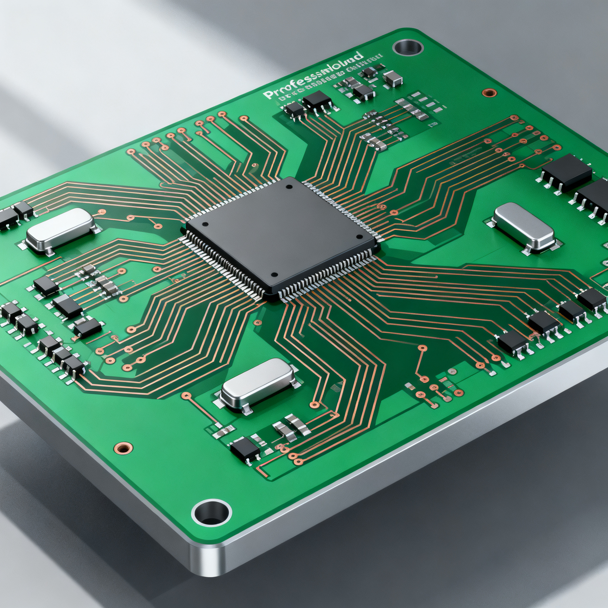
PCB design and manufacturing involve a complex interplay of various technical factors, each impacting the overall production timeline. The core concepts include PCB layout rules, stackup design, signal integrity, and manufacturing considerations. Understanding these principles is vital for minimizing production delays and ensuring high-quality outputs.
PCB layout rules dictate how components are placed and connected on a board. Adhering to these rules helps avoid common pitfalls such as signal interference and manufacturing defects. Stackup design, on the other hand, determines the arrangement of multiple layers within a PCB, impacting both electrical performance and mechanical reliability.
Signal integrity is another critical aspect, ensuring that electrical signals are transmitted without degradation. This involves careful consideration of trace widths, via sizes, and clearances to prevent signal loss or distortion. Finally, manufacturing considerations encompass the selection of suitable materials and processes that align with design requirements and production capabilities.
Detailed Specifications
When designing a PCB, certain specifications are paramount to ensure both functionality and manufacturability. These include trace width, spacing, via sizes, and clearances, which collectively influence the board's electrical performance and structural integrity. Adhering to these specifications not only facilitates efficient manufacturing but also reduces the likelihood of errors and rework.
| Design Parameter | Minimum Value | Recommended Value |
|---|---|---|
| Trace Width | 0.1 mm | 0.2 mm |
| Trace Spacing | 0.1 mm | 0.15 mm |
| Via Diameter | 0.2 mm | 0.3 mm |
| Via Hole Size | 0.1 mm | 0.2 mm |
| Annular Ring | 0.05 mm | 0.1 mm |
| Pad Size | 0.3 mm | 0.5 mm |
| Clearance to Edge | 0.2 mm | 0.3 mm |
| Silkscreen Clearance | 0.1 mm | 0.2 mm |
| Solder Mask Clearance | 0.05 mm | 0.1 mm |
| Minimum Drill Size | 0.15 mm | 0.25 mm |
Key Takeaways from the Specifications
The specifications outlined in the table highlight the importance of adhering to precise design parameters. Proper trace width and spacing are critical for maintaining signal integrity and preventing crosstalk. Similarly, appropriate via sizes and clearances ensure reliable electrical connections and ease of manufacturing. By following these guidelines, designers can create robust PCBs that meet both performance and production requirements, ultimately reducing lead times and minimizing the risk of costly redesigns.
| Layer Configuration | Layer Count | Applications |
|---|---|---|
| Single Layer | 1 | Simple, low-cost circuits |
| Double Layer | 2 | Basic consumer electronics |
| Four Layer | 4 | Complex digital circuits |
| Six Layer | 6 | High-speed applications |
| Eight Layer | 8 | Advanced RF designs |
| Ten Layer | 10 | High-density interconnects |
| Twelve Layer | 12 | High-performance computing |
Practical Implications
The choice of layer stackup is a crucial design decision that affects both the electrical performance and manufacturability of the PCB. Single-layer boards are cost-effective for simple circuits, while multi-layer configurations support complex designs with improved signal integrity and reduced electromagnetic interference. Understanding the applications and benefits of each stackup option allows designers to select the most suitable configuration for their specific project needs, balancing performance requirements with production costs.
| Material | Dielectric Constant (Dk) | Loss Tangent |
|---|---|---|
| FR-4 | 4.2-4.7 | 0.02 |
| Rogers 4350B | 3.48 | 0.0037 |
| Rogers 4003C | 3.38 | 0.0027 |
| Isola FR408 | 3.75 | 0.009 |
| Nelco N7000-2 | 3.6 | 0.010 |
| Arlon 85N | 3.5 | 0.0045 |
| DuPont Pyralux | 3.5 | 0.0025 |
| Panasonic Megtron 6 | 3.7 | 0.003 |
| Ventec VT-47 | 4.0 | 0.005 |
| Shengyi S1000-2 | 4.2 | 0.006 |
Application Guidelines
The choice of PCB materials significantly impacts the board's performance, particularly in high-frequency applications. Materials like FR-4 are versatile and widely used due to their balance of cost and performance. However, for applications requiring superior signal integrity, materials such as Rogers 4350B or DuPont Pyralux offer lower dielectric constants and loss tangents, making them ideal for RF and microwave circuits. Selecting the appropriate material based on dielectric properties and application requirements ensures optimal performance and reliability in the final product.
Design Considerations
When designing a PCB, several practical guidelines must be considered to ensure both manufacturability and performance. First, designers should prioritize simplicity and clarity in the layout to facilitate easier manufacturing and testing. This includes minimizing the number of vias and trace layers where possible, as each additional layer adds complexity and cost.
Signal integrity must be a top priority, particularly in high-speed applications. This involves careful consideration of trace lengths, impedance matching, and the use of proper termination techniques to prevent signal reflections. Additionally, designers should pay attention to power distribution networks (PDNs) to ensure stable power delivery across the board.
Thermal management is another critical aspect, as excessive heat can degrade performance and reduce reliability. Incorporating thermal vias, heat sinks, and proper copper fills can help dissipate heat effectively. Finally, compliance with industry standards such as IPC-A-610 and IPC-2221 is essential for ensuring quality and consistency in the final product.
Step-by-Step Implementation
- Define Requirements: Begin by clearly defining the project's requirements, including electrical, mechanical, and environmental specifications.
- Choose Materials: Select appropriate materials based on dielectric properties, thermal performance, and cost considerations.
- Design Stackup: Determine the layer configuration that best meets the project's needs, balancing performance with manufacturability.
- Layout the PCB: Use CAD tools to place components and route traces, adhering to design rules for trace width, spacing, and clearances.
- Simulate and Analyze: Conduct signal integrity and thermal simulations to identify potential issues and optimize the design.
- Review and Verify: Perform a thorough design review to ensure compliance with industry standards and project requirements.
- Generate Manufacturing Files: Create Gerber files, drill files, and assembly drawings necessary for production.
- Collaborate with Manufacturers: Work closely with PCB manufacturers to address any design-for-manufacturing (DFM) concerns and finalize production plans.
Common Issues & Solutions
- Issue: Signal Integrity Problems
Solution: Use controlled impedance routing and proper termination techniques. - Issue: Thermal Management Challenges
Solution: Incorporate thermal vias, heat sinks, and copper pours to improve heat dissipation. - Issue: Manufacturing Defects
Solution: Adhere to design rules and collaborate with manufacturers for DFM feedback. - Issue: Delays in Production
Solution: Streamline design processes and maintain open communication with suppliers. - Issue: Component Placement Errors
Solution: Utilize automated placement tools and perform design reviews to catch errors early. - Issue: Cost Overruns
Solution: Optimize design complexity and material selection to balance performance with cost.
Applications & Use Cases
PCBs are integral to a wide range of applications, from consumer electronics to industrial systems. In consumer electronics, PCBs enable the compact design of smartphones, tablets, and wearables, providing the necessary circuitry for advanced features and connectivity. In the automotive industry, PCBs are used in advanced driver-assistance systems (ADAS), infotainment systems, and electronic control units (ECUs), enhancing vehicle safety and functionality.
In industrial and medical applications, PCBs support complex control systems, instrumentation, and diagnostic equipment, ensuring precise operation and reliability. The versatility and adaptability of PCBs make them indispensable across diverse sectors, driving innovation and technological advancement.
Selection & Sourcing Guide
When sourcing PCBs, it's crucial to partner with reputable suppliers who offer high-quality materials and manufacturing capabilities. Consider suppliers that adhere to industry standards and provide comprehensive support throughout the design and production process. For a reliable source of integrated circuits and components, visit IC Online, which offers a wide selection of products to meet various design needs.
FAQ
- Q: How can I reduce PCB production lead times?
A: Optimize design processes, adhere to design rules, and collaborate closely with manufacturers. - Q: What is the importance of signal integrity in PCB design?
A: Signal integrity ensures that electrical signals are transmitted without distortion, crucial for high-speed applications. - Q: How do I choose the right layer stackup for my PCB?
A: Consider the complexity of the design, performance requirements, and cost constraints to select an appropriate stackup. - Q: What materials are best for high-frequency applications?
A: Materials like Rogers 4350B and DuPont Pyralux offer low dielectric constants and loss tangents, ideal for RF applications. - Q: How can I improve thermal management in my PCB design?
A: Use thermal vias, heat sinks, and proper copper fills to enhance heat dissipation. - Q: What are common manufacturing defects in PCBs?
A: Defects can include misaligned components, poor solder joints, and incomplete etching, often due to design or process errors. - Q: How do I ensure compliance with industry standards?
A: Follow guidelines from IPC standards and collaborate with experienced manufacturers to ensure quality. - Q: What role do vias play in PCB design?
A: Vias provide electrical connections between layers, enabling complex routing and signal integrity. - Q: How can I minimize cost overruns in PCB production?
A: Simplify design complexity, select cost-effective materials, and maintain clear communication with suppliers. - Q: What are the benefits of using automated design tools?
A: Automated tools enhance accuracy, reduce design time, and help identify potential issues early in the process.
Conclusion
Reducing PCB production lead times is essential for maintaining competitiveness in the fast-paced electronics industry. By implementing effective design strategies, adhering to industry standards, and collaborating with experienced manufacturers, companies can achieve faster turnaround times while maintaining high-quality outputs. Understanding the critical aspects of PCB design, from layout rules to material selection, enables designers to optimize their processes and deliver innovative solutions that meet market demands.