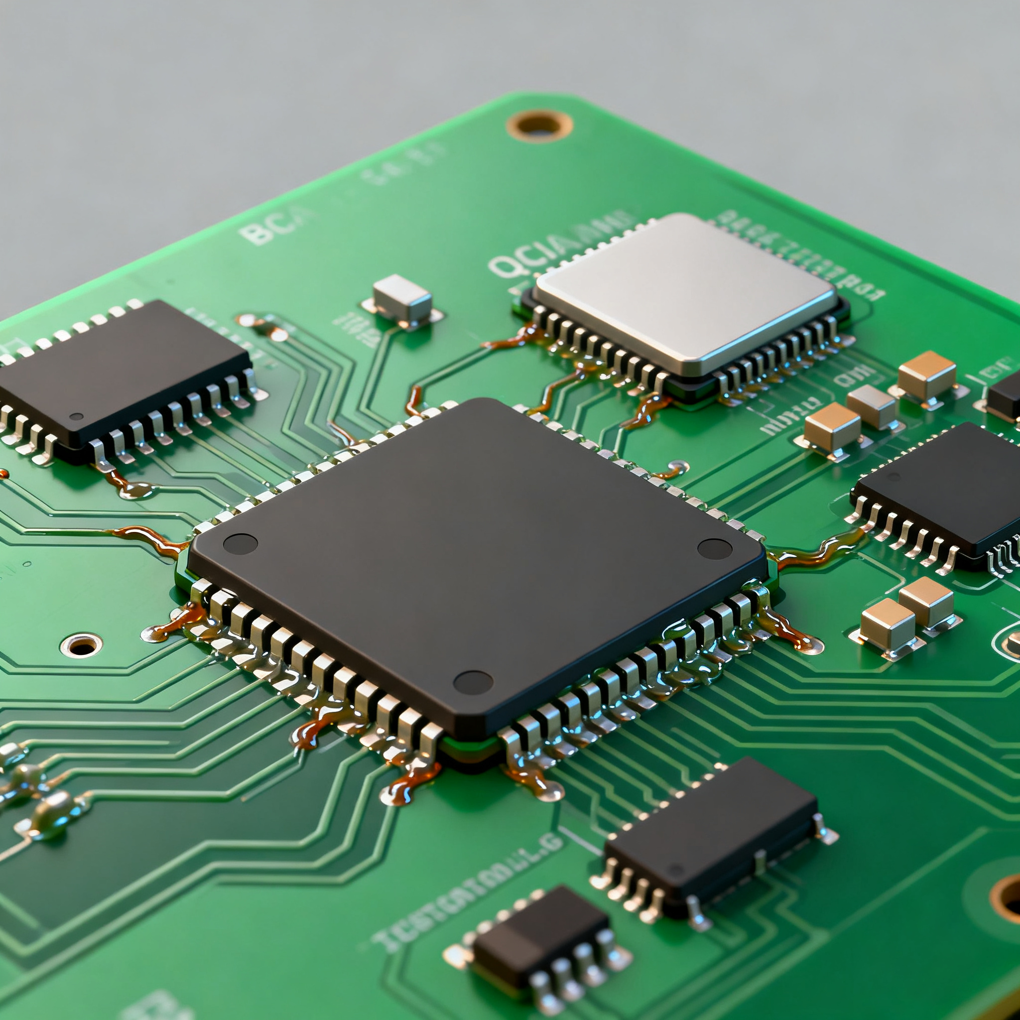
Reduce PCBA Rework Costs by Tackling 5 Soldering Defects: Solder Bridging, Voids, and Tombstoning in BGA & QFN Packages
Why Solder Bridging, Voids, and Tombstoning Spike Rework Costs on Complex BGA & QFN Boards A single bridge across a 0.4 mm-pitch BGA isn't just a localized defect—it's a chain reaction waiting to unfo...
Why Solder Bridging, Voids, and Tombstoning Spike Rework Costs on Complex BGA & QFN Boards
A single bridge across a 0.4 mm-pitch BGA isn't just a localized defect—it's a chain reaction waiting to unfold. When that first board fails AOI and lands in the rework queue, you've already lost more than the cost of a technician's time. Rework on dense BGA and QFN assemblies cascades into pad lifting risks, intermetallic embrittlement, and substrate degradation that can turn a $50 rework job into a scrap decision.
The math is sobering. Even a 2% defect rate on a 5,000-board production run means 100 boards require intervention. If each rework cycle consumes 20–40 minutes of skilled labor plus consumables—solder wick, flux, replacement balls, and possibly a new component—the direct cost per board can range from $25 to over $80. But as Sanshun Smart's cost analysis reveals, the hidden risks of excessive heat excursions are far more damaging. Repeated thermal cycling above 230°C degrades the FR-4 substrate, weakens copper trace adhesion, and grows brittle intermetallic layers that pass electrical test today but fail in the field six months later.
Solder bridging, voids, and tombstoning share a common thread: they rarely originate from operator error alone. These three defect categories are overwhelmingly driven by design decisions made weeks before the first stencil is cut—pad geometries, aperture ratios, paste chemistry, and reflow profile architecture. LCSC's defect overview underscores that understanding the root causes is the prerequisite to effective quality control, not merely inspecting defects out after the oven.
For manufacturing buyers and DFM engineers, the implication is clear: every dollar spent on process optimization and design-for-manufacturing analysis returns multiples in avoided rework, preserved substrate integrity, and field reliability. The following sections dissect the mechanics of these three defect categories, compare capital investment paths, and deliver actionable tuning parameters you can deploy on your next build.
Inside the Solder Joint: How BGA and QFN Geometry Shapes Bridging, Voids, and Tombstoning
Defects don't appear randomly—they follow the physics of molten solder, surface tension, and thermal gradients. Understanding the geometry-specific failure modes for BGA and QFN packages is the foundation for effective prevention.
Solder bridging in BGA packages occurs when excess paste volume or insufficient standoff height allows neighboring balls to merge during reflow. Fine-pitch BGAs at 0.4 mm create capillary conditions where surface tension, rather than pulling solder toward individual pads, forms liquid bridges between adjacent deposits. The root cause typically traces back to stencil aperture design: an area ratio below 0.5 can cause inconsistent paste release, while ratios above 0.8 without adequate gasketing can over-deposit paste. PCBElec's stencil optimization guidelines confirm that aperture ratios between 0.6 and 1.0, paired with laser-cut electropolished walls, provide the paste volume predictability needed for fine-pitch arrays.
Voids in QFN thermal pads are a different beast entirely. The large central slug beneath a QFN package creates an expansive solder interface where flux volatiles struggle to escape before solidification. As the solder melts from the perimeter inward, outgassing flux gets trapped beneath the package body, forming voids that can occupy 15–30% of the thermal pad area if left uncontrolled. These voids aren't cosmetic—they increase thermal resistance from junction to board, pushing component temperatures higher and accelerating electromigration in power devices. AllPCB's ASTM flux activity testing reference highlights how flux chemistry selection and preheat soak duration directly influence outgassing behavior and final void percentage.
Tombstoning—where a chip component stands vertically on one pad—is primarily a wetting force imbalance problem. When one termination reaches liquidus before the other, the surface tension of the molten solder pulls the component upright. This is especially prevalent on 0402 and 0201 passives where thermal mass is low and any asymmetry in pad geometry, copper trace width, or via placement creates a temperature differential across the component body.
The table below maps each defect to its dominant root causes and the rework cost multiplier relative to a clean first-pass board:
| Defect | Dominant Root Causes | Package Types Most Affected | Direct Rework Cost per Board | Hidden Risk Multiplier |
|---|---|---|---|---|
| Solder Bridging | Excess paste volume, poor aperture release, insufficient standoff, aggressive reflow ramp | 0.4–0.5 mm pitch BGA, QFP, fine-pitch QFN | $25–$50 (desolder, clean, reball/reprint) | 2–4× (pad lifting, solder mask damage) |
| Voids (>25% area) | Flux entrapment, rapid liquidus transition, inadequate preheat soak, paste solvent retention | QFN thermal pads, large BGA power balls | $15–$35 (reflow rework, possible reball) | 1.5–3× (thermal degradation, latent delamination) |
| Tombstoning | Uneven pad thermal mass, asymmetric trace widths, via-in-pad without backfill, aggressive ramp rate | 0402, 0201 chip components; occasionally 0603 | $5–$15 (manual reposition, touch-up solder) | 1.2–2× (cracked terminations, lifted pad edge) |
| Insufficient Solder / Head-in-Pillow | Warped BGA substrate, insufficient peak temperature, oxidized ball surface, poor paste tack | Large BGA (>31 mm), PoP stacks, lead-free high-Tg boards | $40–$80+ (full reball, often scrap) | 3–5× (intermetallic fracture, field return) |
Tip: The hidden risk multiplier in the table reflects the probability that rework induces secondary damage—lifted pads, delaminated substrates, or embrittled intermetallic layers—that may pass final test but reduce the board's operational lifespan by 30–50%. When the multiplier exceeds 3×, scrapping the board is often the economically rational choice, especially for Class 3 assemblies.
Selective Soldering vs. Reflow Process Optimization: Where Your Rework Dollar Goes Furthest
When bridging and void defects persist on mixed-technology boards—those combining dense SMT BGA/QFN arrays with through-hole connectors—engineering teams face a capital allocation decision. Should they invest in selective soldering equipment to eliminate manual hand-soldering of through-hole parts, or tighten reflow process controls across the SMT line? The answer depends on where defects actually originate.
Selective soldering excels at eliminating bridging on through-hole connectors where adjacent pins with tight pitch are hand-soldered by operators of varying skill. Aivon's comprehensive ROI analysis demonstrates that selective soldering reduces defects such as bridging and insufficient fill by replacing manual inconsistency with programmable nozzle positioning, precise solder flow control, and reproducible thermal profiles. For boards where through-hole connectors account for 40% or more of total bridging defects, selective soldering payback typically falls under 9 months.
However, if the majority of your defects originate in the SMT reflow zone—BGA bridges, QFN voids, tombstoned chip components—then upgrading reflow oven fidelity and stencil process controls yields a higher return. Modern 10-zone reflow ovens with closed-loop profiling maintain ±1°C uniformity across the conveyor width, enabling the knee-shaped soak profiles that drive flux volatiles out of QFN thermal pads before liquidus. Winwinchip's panel utilization analysis shows that raising first-pass yield through better thermal control and array optimization can cut assembly cost per board by 15–25% by spreading fixed machine-cycle time across more good boards.
The comparison matrix below helps you evaluate which investment path aligns with your defect profile:
| Comparison Metric | Selective Soldering Investment | Reflow Oven & Stencil Process Upgrade | Selection Criteria & Failure Boundary |
|---|---|---|---|
| Primary Defects Addressed | Through-hole bridging, insufficient PTH fill, inconsistent joint volume | BGA bridging, QFN voids, tombstoning, head-in-pillow, graping | Map your last 500 defects: if >40% are PTH-related, selective soldering wins. If SMT dominates, reflow upgrade is priority. |
| Capital Cost Range | $60K–$180K for production-grade selective soldering system | $80K–$250K for 10-zone reflow oven with profiling; $20K–$40K for stencil laser-cutting upgrade | Consider total cost of ownership including nitrogen generation for reflow (adds $15K–$30K). Selective soldering requires dedicated floor space and operator training. |
| Defect Reduction Rate | 70–90% reduction in PTH bridging and insufficient fill (Aivon study) | 50–75% reduction in SMT bridging/void defects with closed-loop control | Reduction rates assume concurrent process optimization—equipment alone without profile tuning yields 40–50% improvement at best. |
| Typical Payback Period | 6–9 months for high-mix through-hole assemblies | 6–12 months for boards with >50% BGA/QFN area ratio | Calculate using avoided rework labor, scrapped board replacement cost, and field return liability. Include the cost of one latent field failure (can exceed $5K in automotive/mil). |
| Scalability | Limited to through-hole; no impact on SMT defect rates | Benefits all SMT components across the panel; synergistic with paste inspection upgrades | For mixed-technology boards, the optimal path is often both—but sequence matters. Fix SMT defects first (larger area of impact), then address PTH-specific issues. |
For most contract manufacturers and OEMs assembling boards with moderate to high BGA/QFN density, the reflow-and-stencil upgrade path delivers broader defect reduction per dollar invested. The exception is high-mix, low-volume production where through-hole connectors dominate the component count and manual soldering variability is the primary defect generator.
Design and Process Moves That Prevent Defects Before the Oven: Stencil, Paste, and Profile Tuning
Prevention isn't a slogan—it's a set of parameter choices that determine whether your first-pass yield lands at 92% or 99.5%. The difference between those two numbers, on a 10,000-board annual volume, is 750 boards that either ship clean or cycle through rework. Sanshun Smart's prevention-first FPY approach drives home the point: optimizing the pick-and-place and stencil process upstream is the only reliable path to high first-pass yield. Every rework touch adds risk.
Stencil Design for Fine-Pitch Defect Elimination
The stencil is your first and most powerful defense against bridging. For 0.4 mm-pitch BGAs, specifying a 100 µm (4 mil) laser-cut stencil with electropolished aperture walls achieves the area ratio needed for consistent paste release. Electropolishing removes the microscopic burrs left by laser cutting, reducing paste adhesion to the aperture walls and ensuring each deposit matches its target volume. PCBElec's stencil optimization guidelines confirm that an area ratio of 0.6–0.8, combined with electropolished walls, delivers the controlled paste deposition essential for fine-pitch bridging prevention.
For QFN thermal pads, aperture segmentation is the critical technique. Rather than a single large opening that deposits a monolithic paste brick under the thermal slug, segment the aperture into multiple smaller windows separated by 0.2–0.3 mm webs. This creates escape channels for flux volatiles during reflow, directly reducing void formation. Typical segmentation splits a 4×4 mm thermal pad into a 2×2 or 3×3 grid of smaller paste deposits.
Thermal Profiling That Eliminates Voids and Tombstoning
Ramp rate is the single most influential profile parameter for both tombstoning and void formation. A ramp of 1–3°C per second from ambient to 150°C allows all component bodies—regardless of thermal mass—to heat uniformly. Faster ramps create thermal differentials across 0402 components where the pad connected to a heavy copper plane lags behind the pad tied to a thin signal trace, producing the wetting force imbalance that drives tombstoning.
For void elimination in QFN assemblies, insert a 60–90 second soak zone at 150–170°C before the reflow peak. This "knee-shaped" profile gives flux activators time to fully volatilize solvents and begin oxide reduction before the solder reaches liquidus. When the solder melts, gas evolution is largely complete, and voids are minimized. Peak temperature should target 235–245°C for SAC305 alloys—hot enough for complete wetting, cool enough to avoid excessive intermetallic growth.
Inspection Gates That Catch Escapes
AOI alone cannot verify what hides beneath a QFN package or inside a BGA array. While AOI effectively inspects edge fillets and visible joints, NextPCB's IPC-7711/7721 rework discipline reinforces that process validation requires X-ray inspection for hidden joints. A 2D X-ray system captures void percentage in QFN thermal pads and detects bridging beneath BGA packages. For high-reliability boards, supplement 2D X-ray with periodic cross-section coupon analysis to verify intermetallic thickness and solder joint microstructure.
The table below consolidates the key process parameters that directly reduce bridging, voiding, and tombstoning:
| Process Parameter | Recommended Range | Defect(s) Controlled | Validation Method |
|---|---|---|---|
| Stencil Thickness (fine-pitch BGA) | 100 µm (4 mil) for 0.4 mm pitch; 125 µm (5 mil) for 0.5–0.8 mm pitch | Bridging, insufficient solder | SPI (Solder Paste Inspection) for volume repeatability |
| Stencil Aperture Area Ratio | 0.6–1.0 (area ratio = aperture opening area / aperture wall area) | Bridging, insufficient paste release | Post-print AOI; verify paste transfer efficiency >85% |
| QFN Thermal Pad Aperture Segmentation | Divide into 4–9 sub-apertures with 0.2–0.3 mm webs | Voids >25% area | 2D X-ray: measure void area as % of total pad area |
| Ramp Rate (ambient to 150°C) | 1–3°C/sec; uniform across all board zones | Tombstoning, component cracking | Thermocouple profiling at multiple board locations |
| Soak Duration (150–170°C) | 60–90 seconds minimum for QFN-heavy designs | Voids, flux residue entrapment | Profile verification; X-ray void analysis post-reflow |
| Peak Temperature (SAC305) | 235–245°C; time above 217°C: 45–90 seconds | Head-in-pillow, intermetallic thickness | Profile board at BGA center and QFN thermal pad |
| Cooling Rate | 2–4°C/sec to below 100°C | Intermetallic grain structure, joint strength | Cross-section grain analysis per IPC-7095 |
| Maximum Rework Cycles (IPC-7711/7721) | ≤3 total heat cycles; peak <250°C per cycle | FR-4 degradation, pad lifting | Cross-section coupon after rework qualification |
Tip: Implement Solder Paste Inspection (SPI) as a gate immediately after printing. Catching paste volume deviations before component placement eliminates the downstream cost of reworking populated boards. An SPI system with ±5 µm height resolution can detect the subtle volume variations that produce bridging on 0.4 mm-pitch BGAs, paying for itself within 12–18 months on lines running >5,000 boards annually.
At NovaPCBA, we integrate these process controls as standard for all BGA and QFN assemblies—electropolished stencils, segmented QFN apertures, and closed-loop 10-zone reflow profiling—because we've measured the compounding cost of rework across thousands of production runs. The cheapest rework is the one you never touch.
Six Questions Manufacturing Buyers and DFM Engineers Ask About Reducing Soldering Defects
These questions come from real conversations with engineers managing high-density BGA and QFN production. The answers reflect the intersection of process physics, economic reality, and field reliability data.
Q: How much does reworking a single BGA with solder bridging really cost when we factor in hidden risks like pad lifting?
Direct rework costs—desoldering the BGA, cleaning pads, reballing or replacing the component, and reflowing—range from $15 to $50 per BGA depending on package size and pitch. A 0.4 mm-pitch, 400-ball BGA demands 30–45 minutes of skilled technician time plus consumables. But the hidden costs dwarf the visible ones. Sanshun Smart's analysis highlights that excessive heat excursions degrade the FR-4 substrate, weaken copper-to-prepreg adhesion, and grow brittle intermetallic layers. A lifted pad during rework typically means the board is scrap. Even when pads survive, the cumulative thermal stress of 2–3 rework cycles can create latent opens that manifest months later in the field. When field return costs—diagnostics, replacement, brand damage—are amortized, the true cost of a reworked BGA can exceed $200–$400 per incident. For Class 3 assemblies, the industry consensus is that boards requiring more than one BGA rework should be scrapped.
Q: Can we rely on automated optical inspection (AOI) alone to catch voids in QFN thermal pads, or is X-ray mandatory?
AOI cannot see beneath QFN packages—period. It inspects only the visible edge fillets where the solder wets the package side terminations. The thermal pad, which conducts 70–90% of the heat from a power QFN, sits entirely beneath the package body and is optically invisible. For void detection, 2D X-ray is the minimum viable inspection technology. It captures a top-down density image where voids appear as lighter regions within the darker solder mass. For high-reliability applications—automotive powertrain, aerospace DC-DC converters, medical implant power supplies—3D X-ray or CT scanning provides cross-sectional void distribution data that 2D systems can miss. Cross-section coupon analysis remains the gold standard for process qualification, particularly when verifying that void percentage meets IPC-7095 Class 2 or 3 limits.
Q: What is the typical payback period for upgrading to a 10-zone reflow oven with closed-loop profiling compared to expanding selective soldering capacity?
For boards where BGA and QFN packages occupy more than 50% of the total component area, a 10-zone reflow oven with closed-loop nitrogen-capable profiling reduces bridging and void defects by 50–75% with proper profile tuning. At a capital cost of $80K–$250K, payback through avoided rework labor, scrapped board replacement, and reduced field returns typically lands between 6 and 12 months for volumes exceeding 3,000 boards annually. Selective soldering payback is faster—often under 9 months per Aivon's ROI study—but only when through-hole connectors are the dominant defect source. If your defect Pareto chart shows SMT bridging and BGA voids as the top two categories, the reflow upgrade is the mathematically superior investment. Many mid-volume contract manufacturers sequence these investments: optimized reflow first (broader impact), selective soldering second (targeted PTH improvement).
Q: How does stencil laser-cutting with electropolishing specifically stop bridging on 0.4 mm pitch components?
Bridging on 0.4 mm-pitch BGAs is fundamentally a paste volume control problem. With pad diameters of approximately 0.23 mm and a gap of only 0.17 mm between pads, even a 15% excess in paste volume can cause adjacent deposits to merge during reflow. Laser-cut stencils without electropolishing leave microscopic ridges and burrs along the aperture walls—remnants of the laser ablation process. These surface irregularities grab solder paste particles, creating inconsistent release with each print stroke. Electropolishing smooths the aperture walls to near-mirror finish (<0.2 µm Ra), eliminating the mechanical adhesion sites that cause paste retention. Combined with a 0.6 area ratio (aperture opening area relative to aperture wall area), paste transfer efficiency stabilizes above 85% stroke-to-stroke. The result is uniform, predictable paste volume per deposit—the primary defense against bridging. PCBElec's guidelines confirm that a 100 µm electropolished stencil with optimized area ratios provides the process window needed for fine-pitch BGA reliability.
Q: When tombstoning appears only on a specific 0402 decoupling cap, should we suspect the C0G dielectric or a footprint design issue?
Isolated tombstoning—affecting one specific component location while identical parts elsewhere on the board reflow perfectly—almost always points to footprint design asymmetry, not component material properties. C0G (Class I) dielectrics are thermally stable and do not exhibit the piezoelectric or thermal expansion anomalies that might theoretically contribute to tombstoning. Instead, examine the PCB layout at the affected location. The most common culprits are: (1) one pad connected to a wide copper plane acting as a heat sink while the opposite pad connects to a thin trace, creating a 10–20°C temperature differential during ramp; (2) asymmetric pad widths where the paste deposits have different volumes, producing unequal wetting forces at liquidus; (3) a via placed immediately adjacent to one pad without thermal relief, again creating a local cold spot. Before changing the component, review the Gerber data for pad symmetry, trace width balance, and via placement. A simple fix—adding thermal relief ties or equalizing trace widths—often eliminates the tombstoning without any component substitution.
Q: Which IPC rework and void acceptance standards should I enforce with my EMS partner to avoid latent field failures from heat-damaged FR-4?
Mandate three specific standards in your EMS quality agreement. First, all rework must follow IPC-7711/7721 procedures, with explicit limits: maximum 3 rework cycles per board, peak board surface temperature not exceeding 250°C at any location, and documented dwell time above 217°C for each cycle. Second, for BGA void acceptance, enforce IPC-7095 Level 2 criteria as the minimum threshold: no more than 25% void area in any single non-thermal ball, and no more than 15% void area in any single thermal ball (those directly under the die attach region). For Class 3 assemblies, tighten thermal ball void limits further to 10% maximum. Third, require your EMS partner to provide cross-section coupon evidence from the process qualification build, demonstrating acceptable intermetallic thickness (1–4 µm for SAC305 on ENIG) and confirming no evidence of pad cratering or substrate delamination within the rework simulation samples. ASTM solder testing standards provide the repeatable test methods that underpin these acceptance criteria, reducing variability and improving long-term process control.
Key actionable checklist for buyers and DFM engineers:
- Require SPI data for all stencil-printed boards with 0.5 mm pitch or finer components—paste volume CpK must exceed 1.33 for the production run
- Specify X-ray void analysis sampling rate: 1 board per 50 for Class 2; 1 board per 20 for Class 3 assemblies with QFN thermal pads
- Include rework cycle tracking in your EMS partner's MES or travelers—any board exceeding 2 cycles requires engineering review before further processing
- Add cross-section coupon requirements to the PCBA fabrication drawing: one coupon at panel corner, one near the largest BGA, sampled every 500 boards
- Negotiate defect-based pricing clauses: if bridging or void defects exceed 500 ppm for 3 consecutive lots, the EMS partner funds the root cause investigation and process requalification
References & Further Reading
The following resources informed this article and provide additional technical depth on soldering defect prevention, rework economics, and process optimization standards:
- The True Cost of Reworking PCBA Boards: Hidden Risks & Prevention — Sanshun Smart
- Soldering Defects Are Costing You: Solutions to Minimize Rework — LCSC
- The ROI of Selective Soldering Equipment: A Comprehensive Cost Benefit Analysis — Aivon
- How to Reduce PCB Assembly Costs Without Sacrificing Quality — Winwinchip / Hitop Tech
- How to Solder on PCB: Proven Techniques, Tips, and SMT Best Practices — PCBELEC
- PCBA Rework and Repair Technical Guide: Mastering IPC-7711/7721 — NextPCB
- The Ultimate Guide to ASTM Standards for PCB Soldering and Assembly — AllPCB
- NovaPCBA — Professional BGA and QFN Assembly Services
For high-density BGA and QFN assemblies requiring process-validated defect prevention, NovaPCBA's manufacturing services integrate electropolished stencil technology, closed-loop 10-zone reflow profiling, and 2D/3D X-ray inspection to deliver first-pass yields above 99% on fine-pitch designs. Contact our engineering team to discuss your next build's DFM requirements and receive a process qualification plan tuned to your specific defect reduction goals.