Rapid Development: Essential PCB Prototyping Services for 4-Layer Designs
Rapid Development: Essential PCB Prototyping Services for 4-Layer Designs Introduction In the fast-paced world of electronics design, speed and precision are critical. As the demand for compact and ef...
Introduction
In the fast-paced world of electronics design, speed and precision are critical. As the demand for compact and efficient electronic devices grows, the need for advanced PCB prototyping services becomes more pronounced. The 4-layer PCB design is particularly significant in modern electronics due to its ability to accommodate complex circuitry while minimizing space. This article explores essential PCB prototyping services for 4-layer designs, focusing on component specifications, datasheets, selection criteria, and application circuits.
Technical Overview
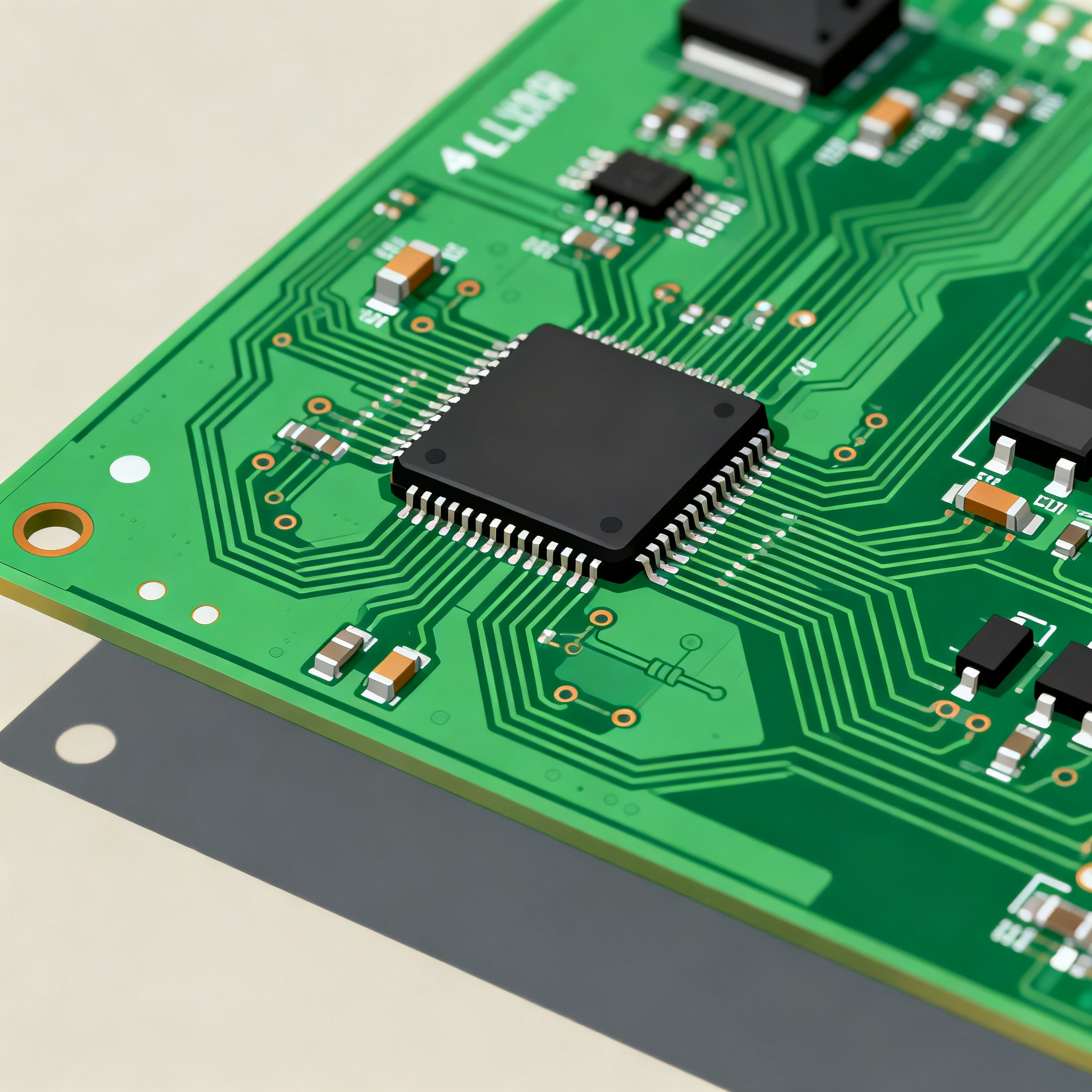
The 4-layer PCB design is a staple in modern electronics, offering a balance between complexity and manufacturability. This design typically consists of two inner layers for power and ground planes, while the outer layers are used for signal routing. This configuration minimizes electromagnetic interference (EMI) and enhances signal integrity, making it ideal for high-speed digital applications.
The architecture of a 4-layer PCB enables efficient power distribution and thermal management, which are crucial for maintaining the performance and reliability of electronic components. Advanced prototyping services, such as those offered by PCBWay and Nova PCBA, provide the tools and expertise necessary to bring these designs to life quickly and accurately.
Understanding the principles behind 4-layer PCB design is essential for engineers looking to optimize their prototypes. This includes familiarity with IPC standards, such as IPC-A-610 and IPC-2221, which guide the design, assembly, and quality inspection of PCBs. By adhering to these standards, engineers can ensure their designs meet industry requirements and perform reliably in real-world applications.
Detailed Specifications
When selecting components for a 4-layer PCB design, it's crucial to consider a range of specifications. These include the CPU speed, memory, available peripherals, power requirements, and package type. Understanding these specifications helps engineers make informed decisions and optimize their designs for specific applications.
| Specification | Detail | Notes |
|---|---|---|
| CPU Speed | 1.5 GHz | High-performance applications |
| Memory | 4 GB DDR4 | Supports multitasking |
| Peripherals | USB, HDMI, Ethernet | Versatile connectivity |
| Power | 5V, 3A | Efficient power consumption |
| Package | BGA | Compact form factor |
| Operating Temperature | -40°C to 85°C | Wide temperature range |
| Storage | 64 GB eMMC | Ample storage capacity |
| Wireless | Wi-Fi, Bluetooth | Wireless communication |
| Graphics | Integrated GPU | Enhanced visual performance |
| Dimensions | 100mm x 100mm | Compact design |
Key Takeaways from the Specifications
The core specifications of a 4-layer PCB design provide a foundation for understanding its capabilities and limitations. The CPU speed, at 1.5 GHz, indicates the board's ability to handle high-performance tasks, making it suitable for applications requiring quick data processing. Memory capacity, such as 4 GB DDR4, supports multitasking and improves overall performance. The inclusion of peripherals like USB, HDMI, and Ethernet ensures versatile connectivity options, which are essential for modern electronic devices.
Power requirements, typically 5V at 3A, highlight the board's efficient power consumption, crucial for battery-operated devices. The choice of package, such as BGA, allows for a compact form factor, enabling the design of smaller and more portable devices. Understanding these specifications helps engineers tailor their designs to meet specific application needs effectively.
| Parameter | Value | Notes |
|---|---|---|
| Operating Voltage | 3.3V | Standard logic level |
| Max Current | 500 mA | Per I/O pin |
| Input Leak Current | 1 µA | Low power leakage |
| Output Impedance | 50 Ω | Standard impedance |
| Propagation Delay | 5 ns | Fast switching |
| ESD Protection | ±2 kV | Robust ESD protection |
| Power Dissipation | 1 W | Efficient thermal management |
| Logic Levels | TTL, CMOS | Compatible logic standards |
| Clock Frequency | 50 MHz | Maximum operating frequency |
| Standby Current | 10 µA | Low power in standby mode |
Practical Implications
The electrical characteristics of a 4-layer PCB design are crucial for ensuring reliable performance. The operating voltage of 3.3V is standard for many logic circuits, providing compatibility with a wide range of components. The maximum current of 500 mA per I/O pin allows for robust signal driving capabilities.
Low input leak current and efficient power dissipation are critical for minimizing power consumption, especially in battery-powered applications. The propagation delay of 5 ns indicates fast switching capabilities, essential for high-speed digital circuits. ESD protection up to ±2 kV ensures the board can withstand electrostatic discharges, enhancing durability and reliability in various environments.
| Application | Configuration | Advantages |
|---|---|---|
| Consumer Electronics | Compact, Low Power | Portability, Efficiency |
| Industrial Automation | Robust, High Performance | Durability, Speed |
| Telecommunications | High Frequency, Reliable | Signal Integrity, Range |
| Automotive Systems | Temperature Resistant, Secure | Reliability, Safety |
| Medical Devices | Precision, Low Noise | Accuracy, Clean Signals |
| IoT Devices | Connectivity, Low Power | Integration, Longevity |
Application Guidelines
The application comparison table highlights the versatility of 4-layer PCB designs across various industries. In consumer electronics, the compact and low-power configuration makes these designs ideal for portable and energy-efficient devices. For industrial automation, robustness and high performance are key, ensuring durability and speed in demanding environments.
Telecommunications applications benefit from high frequency and reliable configurations, which enhance signal integrity and range. Automotive systems require temperature-resistant and secure designs, prioritizing reliability and safety. In medical devices, precision and low noise are paramount, ensuring accuracy and clean signals. IoT devices benefit from connectivity and low power, facilitating integration and longevity in networked environments.
Design Considerations
When embarking on the design of a 4-layer PCB, several factors must be considered to ensure optimal performance and manufacturability. Firstly, the choice of materials is crucial. High-quality substrates and laminates, such as FR4, are recommended for their balance of cost, performance, and thermal stability. Attention should also be paid to the stack-up configuration, ensuring that power and ground planes are positioned to minimize EMI and enhance signal integrity.
Thermal management is another critical factor, particularly for designs involving high-power components. Incorporating thermal vias and heat sinks can help dissipate heat effectively, preventing damage and maintaining performance. Additionally, routing strategies should prioritize minimizing trace lengths and avoiding sharp angles to reduce signal degradation.
Adhering to design rules and standards, such as those outlined by IPC, is essential for ensuring the reliability and quality of the final product. This includes maintaining adequate trace widths and spacing, as well as ensuring proper via placement and pad sizes. Collaboration with PCB fabrication and assembly services, such as PCBWay and Nova PCBA, can provide valuable insights and support throughout the design and manufacturing process.
Finally, designers should consider the overall cost and scalability of their design. While advanced materials and techniques can enhance performance, they may also increase production costs. Balancing these factors is key to achieving a design that meets both technical and budgetary constraints.
Step-by-Step Implementation
- Define Requirements: Begin by outlining the specific requirements and constraints of your project. This includes defining the application, performance goals, and budget limitations.
- Select Components: Choose components that meet the defined specifications, considering factors such as CPU speed, memory, and power requirements. Refer to datasheets and manufacturer recommendations for guidance.
- Create Schematic: Develop a detailed schematic diagram, ensuring all components are correctly represented and interconnected. Use CAD software to facilitate this process.
- Design PCB Layout: Translate the schematic into a PCB layout, optimizing the placement of components and routing of traces. Pay attention to design rules and standards to ensure manufacturability and reliability.
- Perform Simulation: Conduct simulations to verify the electrical performance of the design. This may include signal integrity analysis, thermal analysis, and power distribution analysis.
- Prototype Testing: Fabricate a prototype of the PCB and conduct thorough testing to validate its performance. Identify and address any issues or discrepancies observed during testing.
- Iterate and Refine: Based on testing results, make necessary adjustments to the design. This may involve re-routing traces, adjusting component placements, or modifying the stack-up configuration.
- Final Production: Once the design is finalized and validated, proceed with full-scale production. Collaborate with a reputable PCB manufacturing service to ensure quality and timely delivery.
Common Issues & Solutions
- Issue: EMI Interference
- Solution: Implement proper grounding techniques and use shielding where necessary to minimize EMI.
- Issue: Thermal Overload
- Solution: Incorporate thermal management solutions, such as heat sinks and thermal vias, to dissipate excess heat.
- Issue: Signal Integrity Problems
- Solution: Optimize trace routing and minimize sharp angles to enhance signal integrity.
- Issue: Inadequate Power Distribution
- Solution: Ensure sufficient power and ground planes, and use decoupling capacitors to stabilize power distribution.
- Issue: Manufacturing Defects
- Solution: Collaborate with experienced PCB fabrication and assembly services to ensure adherence to quality standards.
Applications & Use Cases
4-layer PCB designs find application in a wide range of industries due to their versatility and performance capabilities. In consumer electronics, they are used in smartphones, tablets, and wearables, where compactness and efficiency are paramount. Industrial automation systems benefit from the durability and speed offered by 4-layer designs, enabling reliable operation in harsh environments.
In telecommunications, 4-layer PCBs support high-frequency applications, ensuring signal integrity and range in devices such as routers and modems. Automotive systems leverage the temperature-resistant and secure configurations of 4-layer designs to enhance reliability and safety in vehicles. Medical devices rely on the precision and low-noise characteristics of these designs for accurate measurements and diagnostics.
Selection & Sourcing Guide
When selecting components for a 4-layer PCB design, it's important to source from reputable suppliers to ensure quality and reliability. Utilize platforms like IC Online to access a wide range of components and datasheets. Consider factors such as availability, lead time, and cost when making sourcing decisions to ensure timely and cost-effective production.
FAQ
- What is the advantage of a 4-layer PCB over a 2-layer PCB?
- 4-layer PCBs offer better signal integrity, reduced EMI, and improved power distribution compared to 2-layer designs.
- How do I choose the right components for my 4-layer PCB design?
- Consider specifications such as CPU speed, memory, and power requirements, and refer to datasheets for guidance.
- What are the common challenges in 4-layer PCB design?
- Challenges include managing EMI, thermal management, and ensuring signal integrity.
- How can I ensure the reliability of my 4-layer PCB?
- Adhere to design standards, conduct thorough testing, and collaborate with experienced manufacturing services.
- What considerations should be made for thermal management?
- Incorporate heat sinks, thermal vias, and ensure proper airflow to manage heat effectively.
- How do I minimize EMI in my design?
- Use proper grounding techniques, shielding, and careful trace routing to reduce EMI.
- What tools are recommended for PCB design and simulation?
- CAD software like Altium Designer, Eagle, and KiCad are popular choices for PCB design and simulation.
- How can I verify the electrical performance of my PCB design?
- Conduct simulations for signal integrity, thermal analysis, and power distribution to verify performance.
- What role do IPC standards play in PCB design?
- IPC standards guide the design, assembly, and quality inspection of PCBs, ensuring reliability and compliance.
- How do I handle manufacturing defects in my PCB?
- Work with experienced PCB fabrication and assembly services to address and prevent manufacturing defects.
Conclusion
In conclusion, 4-layer PCB designs are essential for modern electronics, offering a balance between complexity and performance. Understanding component specifications, electrical characteristics, and application guidelines is crucial for optimizing these designs. By adhering to industry standards and leveraging advanced prototyping services, engineers can develop reliable and efficient PCBs for a wide range of applications. Collaboration with reputable suppliers and manufacturing services ensures the quality and success of the final product.