Preventing PCBA Manufacturing Defects: Key Strategies for High-Quality Production
Preventing PCBA Manufacturing Defects: Key Strategies for High-Quality Production Introduction In the world of electronics, the reliability and performance of a product heavily depend on the quality o...
Introduction
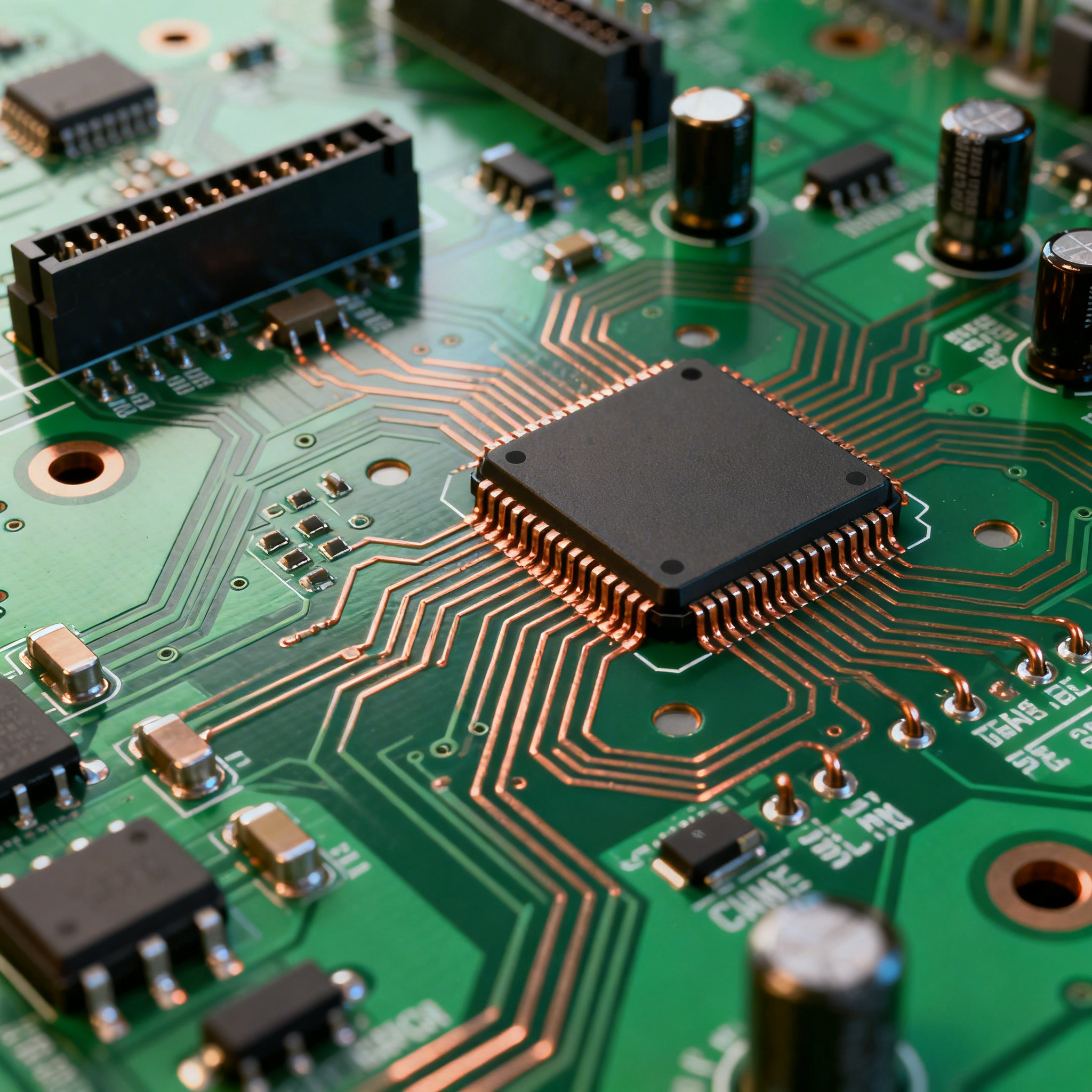
In the world of electronics, the reliability and performance of a product heavily depend on the quality of its printed circuit board assembly (PCBA). As the backbone of electronic devices, PCBs need to be meticulously designed and manufactured to avoid defects that can lead to costly recalls and failures. This article delves into the strategies essential for preventing PCBA manufacturing defects, focusing on PCB layout rules, stackup design, signal integrity, and manufacturing considerations. These strategies are vital for ensuring high-quality production and meeting industry standards.
Technical Overview
The process of designing and manufacturing PCBs is intricate, involving a multitude of factors that can influence the final product's performance. Core concepts such as signal integrity, impedance control, and thermal management play crucial roles in the PCB design process. Signal integrity ensures that signals on the PCB are transmitted without distortion, while impedance control helps maintain consistent signal paths. Thermal management is critical to dissipate heat generated by components, preventing overheating and ensuring longevity. Adhering to industry standards like IPC-A-610 and IPC-2221 is fundamental in achieving reliable PCBs. These standards provide guidelines on design, assembly, and inspection, ensuring that PCBs meet quality requirements.
Detailed Specifications
Specifications are the foundation of any successful PCB design. They encompass various design rules such as trace width, spacing, via sizes, and clearances, which are critical in determining the board's electrical and mechanical performance. Understanding these specifications is imperative for engineers to create a design that is manufacturable and meets performance criteria.
| Design Rule | Minimum Value | Recommended Value |
|---|---|---|
| Trace Width | 4 mils | 6 mils |
| Trace Spacing | 3 mils | 5 mils |
| Via Diameter | 8 mils | 10 mils |
| Annular Ring | 4 mils | 6 mils |
| Clearance to Edge | 10 mils | 20 mils |
| Hole Size | 10 mils | 14 mils |
| Pad Size | 18 mils | 20 mils |
| Aspect Ratio | 8:1 | 10:1 |
| Silkscreen Clearance | 4 mils | 6 mils |
| Solder Mask Clearance | 4 mils | 6 mils |
| Min. Copper to Board Edge | 10 mils | 15 mils |
Key Takeaways from the Specifications
The specifications outlined in the table are crucial for ensuring manufacturability and reliability of the PCB. For instance, maintaining appropriate trace width and spacing is vital for managing current carrying capacity and preventing short circuits. The via and pad sizes influence the mechanical stability and electrical connectivity of the board. Designers must adhere to these specifications to avoid issues such as impedance mismatch and signal loss, which can degrade the performance of the PCB. By following these guidelines, engineers can create designs that are both functional and manufacturable, reducing the risk of defects in the final product.
| Layer Configuration | Number of Layers | Applications |
|---|---|---|
| Single Layer | 1 | Simple circuits, low-cost applications |
| Double Layer | 2 | Consumer electronics, basic RF applications |
| Four Layer | 4 | Multilayer designs, improved signal integrity |
| Six Layer | 6 | Complex designs, enhanced power distribution |
| Eight Layer | 8 | High-speed data transmission, advanced computing |
| Ten Layer | 10 | Data centers, telecommunications |
| Twelve Layer | 12 | High-density interconnects, aerospace |
Practical Implications
The choice of layer stackup configuration is pivotal in determining the PCB's performance and application. A single-layer PCB is suitable for simple, low-cost applications, while multi-layer configurations are essential for more complex designs requiring improved signal integrity and power distribution. As the number of layers increases, so does the PCB's ability to handle high-speed data transmission and complex routing requirements. Designers must carefully consider the application's needs when selecting the appropriate layer configuration to ensure optimal performance and cost-effectiveness.
| Material | Dielectric Constant (Dk) | Loss Tangent (Df) |
|---|---|---|
| FR-4 | 4.2-4.8 | 0.019-0.022 |
| Rogers 4350B | 3.48 | 0.0037 |
| Rogers 5880 | 2.20 | 0.0009 |
| Isola 370HR | 4.04 | 0.019 |
| Nelco N7000 | 3.7 | 0.008 |
| DuPont Pyralux | 3.5 | 0.004 |
| Panasonic Megtron 6 | 3.4 | 0.002 |
| Arlon 85N | 3.5 | 0.004 |
| Polyimide | 3.5-4.0 | 0.004-0.009 |
Application Guidelines
Material selection for PCBs is crucial as it impacts the board's electrical performance and thermal management. FR-4 is a common choice for general applications due to its balanced properties and cost-effectiveness. For high-frequency applications, materials like Rogers 4350B and 5880 offer lower dielectric constants and loss tangents, ensuring minimal signal loss. The choice of material should align with the application's requirements, considering factors such as signal speed, environmental conditions, and budget constraints. By selecting the appropriate material, designers can enhance the PCB's performance and reliability in its intended application.
Design Considerations
Designing a PCB involves several considerations that go beyond the specifications and material choices. Engineers must account for factors such as thermal management, electromagnetic interference (EMI), and manufacturability. Effective thermal management is crucial for preventing component overheating and ensuring long-term reliability. EMI can be mitigated by proper grounding and shielding techniques, essential for maintaining signal integrity. Manufacturability considerations include panelization, testability, and assembly processes, which influence the production yield and cost. By addressing these factors during the design phase, engineers can create robust PCBs that meet performance and quality standards.
Step-by-Step Implementation
Implementing a PCB design from concept to production involves several critical steps:
- Define Requirements: Clearly outline the project's objectives, specifications, and constraints.
- Schematic Design: Create a detailed schematic capturing all components and their interconnections.
- Component Selection: Choose components based on performance, availability, and cost.
- PCB Layout: Design the PCB layout, adhering to design rules and considering signal integrity and thermal management.
- Prototype Fabrication: Manufacture a prototype to validate the design and identify any issues.
- Testing and Validation: Conduct thorough testing to ensure the PCB meets all functional and performance criteria.
- Design Iteration: Refine the design based on test results and feedback, addressing any identified issues.
- Production and Assembly: Finalize the design for mass production, ensuring all processes are optimized for quality and efficiency.
Common Issues & Solutions
Despite careful design and planning, issues can arise during PCB manufacturing. Here are some common problems and their solutions:
- Signal Integrity Issues: Use controlled impedance traces and proper termination techniques to prevent signal distortion.
- Thermal Management Problems: Implement heat sinks, thermal vias, and proper component placement to dissipate heat effectively.
- EMI Interference: Employ shielding and grounding strategies to minimize electromagnetic interference.
- Manufacturing Defects: Conduct thorough design rule checks (DRC) and follow IPC standards to reduce defects.
- Component Misalignment: Use precise pick-and-place machines and proper alignment techniques during assembly.
- Insufficient Testing: Implement comprehensive testing protocols, including in-circuit testing (ICT) and functional testing, to ensure quality.
Applications & Use Cases
PCBs are used in a wide range of applications, from consumer electronics to industrial equipment. In consumer electronics, PCBs enable the compact and efficient design of smartphones, laptops, and wearables. In industrial settings, PCBs are integral to automation systems, providing reliable control and communication. The automotive industry relies on PCBs for advanced driver-assistance systems (ADAS) and infotainment systems. PCBs are also crucial in telecommunications, supporting high-speed data transmission and connectivity. These applications demonstrate the versatility and importance of PCBs in modern technology.
Selection & Sourcing Guide
When selecting and sourcing PCBs, engineers should consider factors such as material properties, manufacturing capabilities, and supplier reliability. Websites like IC Online provide valuable resources for sourcing components and PCBs, offering a wide range of options to meet diverse needs. Working with reputable suppliers ensures quality and timely delivery, essential for successful project execution.
FAQ
- What is the importance of trace width in PCB design? Trace width determines the current-carrying capacity and affects signal integrity. Proper trace width ensures reliable performance.
- How does layer stackup impact PCB performance? Layer stackup influences signal integrity, power distribution, and thermal management, affecting overall performance.
- Why are material properties critical in PCB selection? Material properties like dielectric constant and loss tangent impact signal speed and loss, affecting the PCB's performance.
- What are common causes of PCB manufacturing defects? Common causes include poor design, inadequate testing, and non-compliance with standards. Addressing these can reduce defects.
- How can signal integrity issues be mitigated? Use controlled impedance traces, proper termination, and grounding techniques to maintain signal integrity.
- What role does thermal management play in PCB design? Thermal management prevents overheating, ensuring component reliability and longevity.
- How is EMI reduced in PCB designs? EMI can be reduced through shielding, grounding, and proper component placement.
- What testing methods are used for PCBs? Common testing methods include in-circuit testing (ICT), functional testing, and automated optical inspection (AOI).
- Why is adherence to IPC standards important? IPC standards ensure quality, reliability, and consistency in PCB design and manufacturing.
- What factors should be considered when selecting a PCB supplier? Consider material quality, manufacturing capabilities, lead times, and supplier reputation.
Conclusion
Preventing PCBA manufacturing defects requires a comprehensive approach that includes adhering to design rules, selecting appropriate materials, and considering practical design implications. By following industry standards and implementing effective strategies, engineers can ensure high-quality PCB production, enhancing the reliability and performance of electronic devices. The key is to address potential issues during the design phase, ensuring that the final product meets both functional and quality expectations.
``` This article provides a comprehensive overview of strategies to prevent PCBA manufacturing defects, with detailed tables and practical insights into PCB design and manufacturing considerations.