Preventing PCB Design Errors: Top 10 Tips and Common Pitfalls to Avoid
Preventing PCB Design Errors: Top 10 Tips and Common Pitfalls to Avoid Introduction In the rapidly evolving world of electronics, Printed Circuit Board (PCB) design is a critical component that bridge...
Introduction
In the rapidly evolving world of electronics, Printed Circuit Board (PCB) design is a critical component that bridges the gap between conceptual designs and physical products. As technology advances, the complexity of PCB design increases, making it essential to focus on preventing errors that can lead to costly revisions and delays. This article aims to provide valuable insights into avoiding common pitfalls in PCB design, focusing on circuit topology, component calculations, performance analysis, and design trade-offs.
Technical Overview
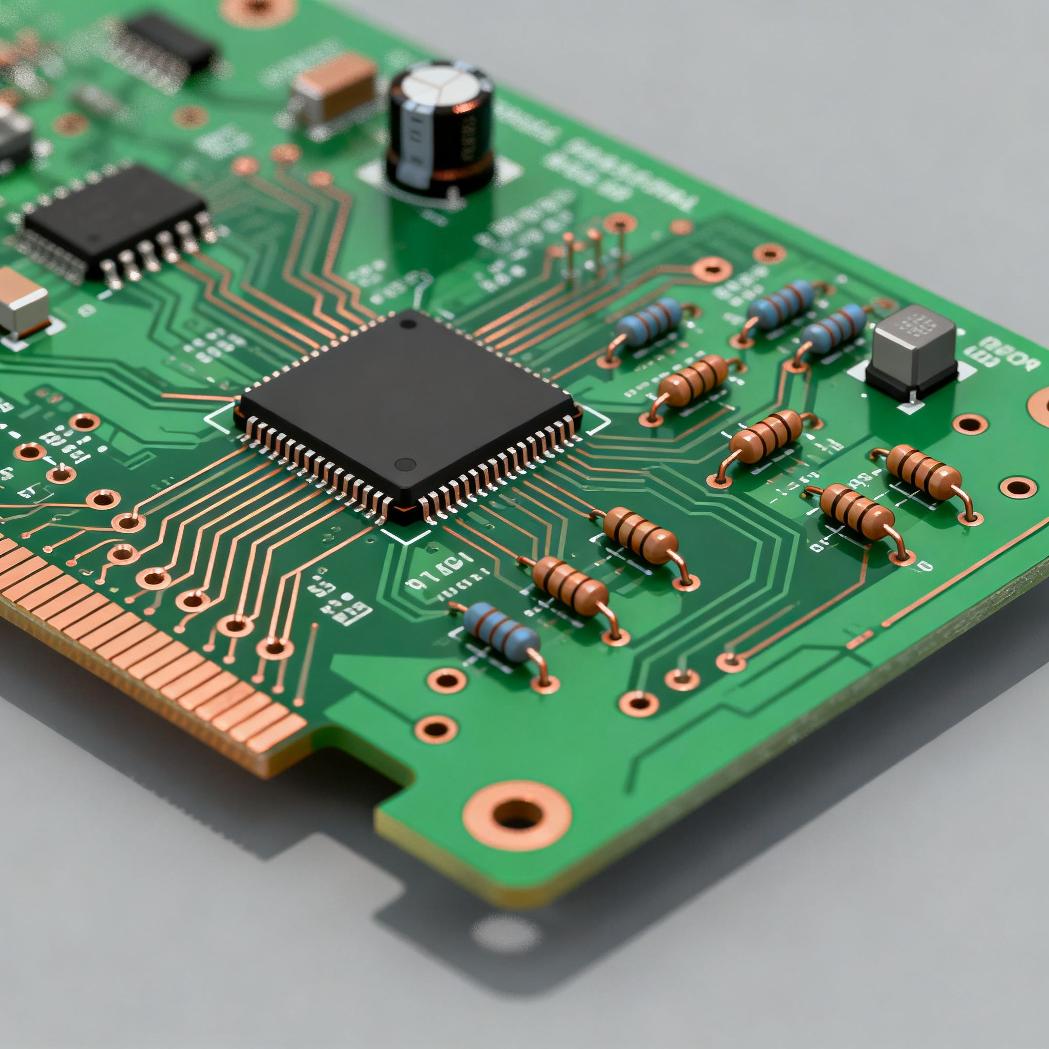
The foundation of successful PCB design lies in understanding the core concepts and principles that govern circuit functionality. Circuit topology, which refers to the arrangement of elements in a circuit, plays a crucial role in determining the electrical performance of the PCB. Careful consideration of component values, placement, and connectivity ensures that the design meets the required specifications. Furthermore, performance analysis is imperative to assess parameters such as gain, bandwidth, noise, and power consumption. Design trade-offs often involve balancing these parameters to achieve optimal performance while keeping costs in check. This technical overview sets the stage for a deeper dive into the detailed specifications and practical guidelines for preventing PCB design errors.
Detailed Specifications
Specifications are the blueprint for any PCB design, defining the electrical, mechanical, and environmental criteria that the design must meet. They are essential for ensuring that the final product functions as intended and complies with industry standards. Key specifications include component values, calculations, and formulas, which are crucial for accurate circuit design and performance. Understanding these parameters helps in making informed decisions during the design process.
| Component | Value | Formula/Calculation |
|---|---|---|
| Resistor | 10kΩ | Ohm's Law: V = IR |
| Capacitor | 100nF | Capacitance: C = Q/V |
| Inductor | 10μH | Inductance: V = L(di/dt) |
| Op-Amp Gain | 100 | Gain: A = Vout/Vin |
| Voltage Divider | 5V output | Vout = Vin(R2/(R1+R2)) |
| RC Time Constant | 1ms | τ = RC |
| Power Supply | 12V | Power: P = VI |
| LED Forward Current | 20mA | I = V/R |
| Transistor Beta | 100 | β = Ic/Ib |
| Filter Cutoff Frequency | 1kHz | f_c = 1/(2πRC) |
Key Takeaways from the Specifications
The specifications table provides a comprehensive overview of essential component values and calculations that form the backbone of PCB design. Understanding these parameters is vital for ensuring the circuit's functionality and reliability. For example, calculating the RC time constant helps in determining the response time of filters, while the gain formula is crucial for designing amplifiers. By adhering to these specifications, designers can avoid common pitfalls such as incorrect component selection and insufficient power supply design, which can lead to performance issues. These specifications serve as a guideline for optimizing the design process and achieving desired circuit performance.
| Parameter | Value | Impact |
|---|---|---|
| Gain | 100 | Amplifies weak signals |
| Bandwidth | 20MHz | Determines signal frequency range |
| Noise | 1nV/√Hz | Affects signal clarity |
| Power Consumption | 500mW | Impacts thermal management |
| Signal Integrity | High | Ensures reliable data transmission |
| Temperature Range | -40°C to 85°C | Defines operating conditions |
| Efficiency | 85% | Reduces energy wastage |
| Latency | 5ns | Affects real-time applications |
| EMI | Low | Minimizes interference |
Practical Implications
The performance analysis table highlights the critical parameters that influence a PCB's operational efficiency. Gain and bandwidth are particularly important for applications requiring signal amplification and wide frequency range coverage. Low noise levels contribute to signal clarity, essential for high-fidelity audio and precision measurements. Power consumption impacts the thermal management strategy, while efficiency influences overall energy usage. Understanding these parameters allows designers to make informed trade-offs to optimize performance. For instance, increasing bandwidth may result in higher noise levels, necessitating additional filtering. These practical implications guide the design process, ensuring the final product meets the intended application requirements.
| Configuration | Pros | Cons |
|---|---|---|
| Single-Layer PCB | Low cost, simple design | Limited routing space |
| Double-Layer PCB | Increased routing options | Higher cost than single-layer |
| Multilayer PCB | High density, complex designs | Expensive, complex manufacturing |
| SMD Components | Compact, automated assembly | Requires precise placement |
| Through-Hole Components | Strong mechanical bonds | Larger, manual assembly |
| Flexible PCB | Flexible, lightweight | Costly, limited material choices |
| Rigid-Flex PCB | Combines rigidity and flexibility | Complex design, high cost |
Application Guidelines
The design trade-offs table presents various PCB configurations and their respective advantages and disadvantages. Choosing the right configuration depends on the specific application and design requirements. Single-layer PCBs are cost-effective for simple designs, while multilayer PCBs cater to high-density and complex circuits. Surface-mount devices (SMD) are ideal for compact designs but require precise placement, whereas through-hole components provide robust mechanical connections. Flexible and rigid-flex PCBs offer unique benefits for applications requiring bending and weight reduction. By understanding these trade-offs, designers can select the most appropriate configuration to meet their project's needs, balancing cost, performance, and manufacturability.
Design Considerations
Successful PCB design requires careful consideration of various factors to prevent errors and ensure optimal performance. Key considerations include component selection, layout design, and thermal management. Selecting the right components involves evaluating electrical specifications, availability, and cost. The layout design should prioritize signal integrity, minimizing trace lengths and avoiding sharp angles to reduce electromagnetic interference (EMI). Thermal management is crucial for preventing overheating, which can lead to component failure. This involves choosing appropriate materials and incorporating heat sinks or thermal vias. Additionally, adhering to industry standards, such as IPC guidelines, ensures quality and reliability. By addressing these considerations, designers can mitigate potential issues and streamline the manufacturing process.
Step-by-Step Implementation
Implementing a PCB design involves several critical steps to ensure a successful outcome. Here's a detailed guide:
- Requirement Analysis: Define the project's objectives and specifications, including electrical, mechanical, and environmental requirements.
- Schematic Design: Create a detailed schematic diagram, specifying components and their interconnections.
- Component Selection: Choose components based on performance, availability, and cost, ensuring compatibility with the design specifications.
- PCB Layout Design: Design the PCB layout, considering trace routing, component placement, and layer stack-up to optimize signal integrity and thermal management.
- Simulation and Validation: Perform simulations to validate the design, checking for errors and verifying performance against specifications.
- Prototype Fabrication: Manufacture a prototype PCB to test the design in real-world conditions, identifying any issues or areas for improvement.
- Testing and Debugging: Conduct thorough testing to identify and resolve any design flaws or performance issues.
- Final Design Review: Review the design with stakeholders, incorporating feedback and making necessary adjustments before mass production.
Common Issues & Solutions
PCB design is prone to several common issues, but understanding potential solutions can help mitigate these challenges. Here are some typical problems and their fixes:
- Signal Integrity Issues: Ensure proper grounding and minimize trace lengths to reduce noise and interference.
- Insufficient Thermal Management: Use thermal vias and heat sinks to dissipate heat effectively and prevent component overheating.
- Component Mismatches: Double-check component specifications and compatibility during the selection process to avoid mismatches.
- EMI Problems: Implement shielding and proper trace routing to minimize electromagnetic interference.
- Manufacturing Defects: Work closely with manufacturers to ensure adherence to design rules and quality standards.
- Design Rule Violations: Regularly validate the design against industry standards and guidelines to prevent rule violations.
Applications & Use Cases
PCBs are integral to a wide range of applications across various industries. In consumer electronics, they are used in smartphones, tablets, and wearable devices, enabling compact and efficient designs. In the automotive industry, PCBs facilitate advanced driver-assistance systems (ADAS) and infotainment solutions. Industrial applications include automation systems and control panels, where reliability and durability are paramount. Medical devices also rely on PCBs for accurate diagnostics and monitoring, while the aerospace industry demands high-performance PCBs for navigation and communication systems. Understanding these applications helps designers tailor their designs to meet specific industry requirements and performance standards.
Selection & Sourcing Guide
Selecting and sourcing components for PCB design is a critical step that influences the final product's performance and cost. Designers should consider factors such as component availability, lead time, and supplier reputation. Online resources like IC Online provide a comprehensive database of electronic components, offering detailed specifications and pricing information. By leveraging such platforms, designers can streamline the sourcing process, ensuring they have access to the right components at competitive prices.
FAQ
- What is the importance of PCB design standards? PCB design standards, such as those set by IPC, ensure quality, reliability, and manufacturability, reducing the risk of errors and defects.
- How do I choose the right PCB material? Consider factors like thermal conductivity, dielectric constant, and mechanical properties to select a material that meets the design requirements.
- What are the benefits of using simulation tools in PCB design? Simulation tools help validate the design, identifying potential issues and allowing for performance optimization before fabrication.
- How can I minimize EMI in my PCB design? Implement proper grounding, use shielding techniques, and maintain adequate trace spacing to reduce electromagnetic interference.
- What are the challenges of multilayer PCB design? Multilayer PCBs offer increased routing options but require careful consideration of layer stack-up and signal integrity to avoid crosstalk and interference.
- How do I ensure efficient thermal management in my PCB design? Use thermal vias, heat sinks, and appropriate materials to dissipate heat effectively and prevent component damage.
- What factors influence PCB manufacturing costs? Factors include board size, layer count, material type, and complexity of the design, as well as the choice of manufacturer.
- How can I avoid component mismatches in my PCB design? Thoroughly verify component specifications and compatibility during the design phase to prevent mismatches and performance issues.
- What is the role of a design review in PCB development? Design reviews involve stakeholders in evaluating the design, providing feedback, and ensuring that all requirements are met before production.
- How do I handle design rule violations? Regularly validate the design against industry standards and guidelines, making necessary adjustments to comply with design rules.
Conclusion
Preventing PCB design errors is crucial for ensuring the success of electronic products in today's competitive market. By understanding circuit topology, component calculations, and performance analysis, designers can make informed decisions that optimize performance and cost. Adhering to design trade-offs and industry standards further enhances the reliability and manufacturability of the final product. By following the guidelines and insights provided in this article, engineers can navigate the complexities of PCB design, delivering high-quality solutions that meet diverse application needs.