Practical Strategies for PCB Assembly Cost Reduction: Real Examples from Industry Leaders
Practical Strategies for PCB Assembly Cost Reduction: Real Examples from Industry Leaders Introduction In the competitive world of electronics manufacturing, reducing costs while maintaining quality i...
Introduction
In the competitive world of electronics manufacturing, reducing costs while maintaining quality is a crucial challenge. PCB assembly, a critical stage in the manufacturing process, offers significant opportunities for cost reduction. By optimizing component selection and understanding detailed specifications, manufacturers can streamline operations and achieve economic efficiency. This article delves into practical strategies for reducing PCB assembly costs, drawing on real-world examples from industry leaders. We'll explore key component specifications, selection criteria, and application circuits, all backed by industry standards and best practices.
Technical Overview
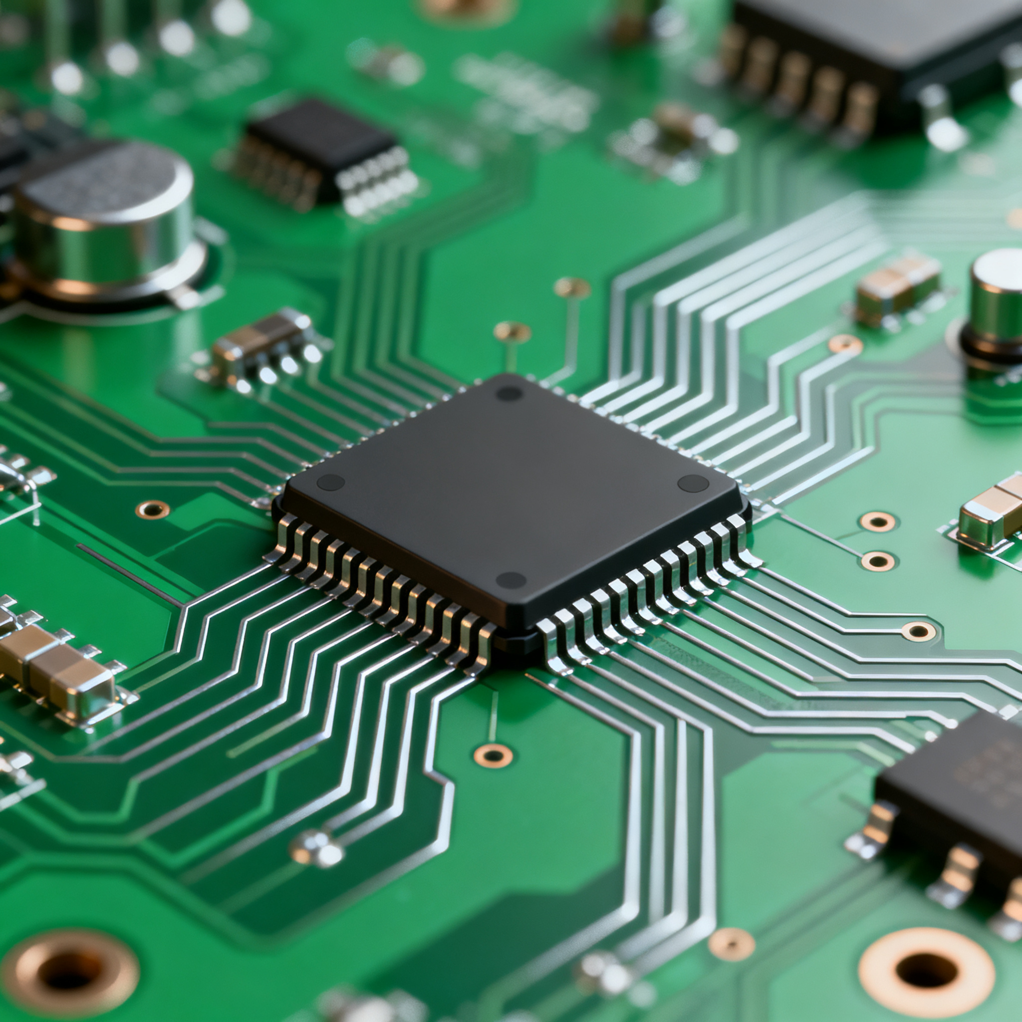
Printed Circuit Boards (PCBs) serve as the backbone of modern electronic devices, providing the necessary support and electrical connections for components. The assembly process involves mounting components onto the PCB, which can be done through surface-mount technology (SMT) or through-hole technology (THT). Each method has its own set of specifications, advantages, and challenges. A deep understanding of the core concepts, such as component placement, signal integrity, and power distribution, is essential for optimizing PCB design and reducing assembly costs.
Industry standards like IPC-A-610 and IPC-2221 provide guidelines for PCB design and manufacturing, ensuring quality and reliability. These standards help in defining the architecture and principles of PCB assembly, including aspects like trace width, spacing, and solder mask requirements. By adhering to these standards, manufacturers can minimize errors and rework, leading to cost savings and improved efficiency.
Detailed Specifications
When it comes to PCB assembly, selecting the right components is crucial. Understanding the core specifications of integrated circuits (ICs) can significantly impact the overall cost and performance of the final product. Key specifications include CPU speed, memory capacity, peripheral interfaces, power requirements, and package type. These factors influence not only the functionality of the device but also the complexity and cost of the assembly process.
| Specification | Details | Importance |
|---|---|---|
| CPU Speed | 1.2 GHz | Determines processing capability |
| Memory | 512 MB RAM | Affects multitasking performance |
| Peripherals | USB, SPI, I2C | Enables external device connectivity |
| Power | 3.3V supply | Impacts energy efficiency |
| Package | LQFP-64 | Influences assembly complexity |
| Temperature Range | -40°C to 85°C | Defines operational environment |
| Storage | Flash 4MB | Determines data retention capability |
| Clock Speed | 32 MHz | Impacts timing precision |
| GPIO Pins | 40 | Allows for versatile interfacing |
| ADC Channels | 8 | Enables analog signal processing |
| Operating Voltage | 1.8V to 3.6V | Ensures compatibility with various components |
Key Takeaways from the Specifications
The data presented in the table highlights the critical specifications that influence the design and functionality of a PCB. CPU speed and memory are pivotal for processing and performance, especially in applications requiring high computational power. The choice of peripherals directly affects the device's ability to interface with other components, impacting overall versatility. Power specifications, including operating voltage and supply requirements, are essential for energy efficiency and compatibility with other components. Understanding these specifications allows engineers to make informed decisions, balancing performance with cost considerations.
| Parameter | Value | Significance |
|---|---|---|
| Operating Voltage | 1.8V to 3.6V | Ensures compatibility with diverse components |
| Max Current | 500 mA | Limits power draw and heat generation |
| Input Voltage Range | 0V to 5V | Determines input tolerance |
| Output Current | 20 mA per pin | Impacts driving capability |
| Timing Jitter | 5 ps | Affects signal integrity |
| Input Capacitance | 5 pF | Influences signal speed |
| Output Voltage | 3.3V | Defines output level |
| Static Power | 100 µW | Impacts idle power consumption |
| Dynamic Power | 200 mW | Relates to power under load |
| ESD Protection | 2 kV | Ensures reliability against electrostatic discharge |
| Leakage Current | 1 µA | Impacts power efficiency |
Practical Implications
The electrical characteristics table provides insights into the component's operational limits and performance. Parameters like operating voltage and max current are crucial for ensuring that components can function effectively within the system's power architecture. Timing jitter and input capacitance are significant for maintaining signal integrity, especially in high-speed applications. Understanding these parameters helps in designing robust and reliable systems that can withstand environmental challenges and electrical stresses, ultimately reducing the risk of failure and associated costs.
| Application | Configuration | Benefits |
|---|---|---|
| Consumer Electronics | Low power, compact design | Cost-effective and energy-efficient |
| Industrial Automation | Robust, high reliability | Durable under harsh conditions |
| Automotive Systems | High temperature range | Reliable in extreme environments |
| Medical Devices | Precision, low noise | Ensures patient safety and accuracy |
| Telecommunications | High-speed data processing | Facilitates rapid connectivity |
| IoT Devices | Low power, wireless capability | Enables remote monitoring |
| Wearable Technology | Compact, battery-efficient | Enhances user comfort |
Application Guidelines
The application comparison table illustrates how different configurations cater to specific industry needs. For instance, consumer electronics prioritize compact and low-power designs to enhance portability and battery life. Industrial automation demands robust and reliable components to withstand demanding environments. Each application has unique requirements, and selecting components that align with these needs is essential for optimizing performance and cost-effectiveness. By understanding the specific benefits of each configuration, engineers can tailor PCB designs to meet the precise demands of the target application.
Design Considerations
Designing a cost-effective PCB assembly involves several critical considerations. First, component selection is paramount; choosing components with the right specifications can prevent unnecessary expenses. Engineers should prioritize components that offer a balance between performance and cost, ensuring they meet the application's requirements without over-specifying.
Another vital aspect is the layout design. Optimizing the PCB layout can reduce material costs and improve manufacturing efficiency. This includes minimizing the number of layers, optimizing trace routing to reduce signal interference, and ensuring adequate spacing to prevent short circuits.
Additionally, considering manufacturing constraints during the design phase can significantly reduce costs. This involves adhering to design for manufacturability (DFM) guidelines, which help streamline the assembly process and minimize errors. Working closely with manufacturers to understand their capabilities and limitations can lead to more efficient designs and cost savings.
Finally, quality control is essential to prevent costly rework and ensure reliability. Implementing rigorous testing procedures and adhering to industry standards can help identify potential issues early, reducing the risk of failures in the field and associated costs.
Step-by-Step Implementation
- Define Requirements: Begin by understanding the application's specific needs and constraints, such as power, size, and environmental conditions.
- Select Components: Choose components that meet the defined requirements, balancing performance and cost. Use datasheets and industry standards to guide selection.
- Design Schematic: Create a detailed schematic that outlines the electrical connections and component interactions.
- Optimize Layout: Design the PCB layout, focusing on efficient trace routing, minimizing layers, and ensuring proper spacing and alignment.
- Review Design: Conduct a thorough review of the design to identify potential issues, such as signal interference or power distribution problems.
- Prototype and Test: Develop a prototype PCB and conduct rigorous testing to validate the design and identify any necessary adjustments.
- Refine and Finalize: Make any necessary adjustments based on testing results and finalize the design for manufacturing.
- Coordinate with Manufacturer: Work closely with the manufacturer to ensure that the design meets their capabilities and constraints, facilitating a smooth production process.
Common Issues & Solutions
- Component Mismatch: Ensure compatibility between components by reviewing datasheets and specifications. Conduct simulations to validate interactions.
- Signal Integrity Problems: Address issues like crosstalk and reflection by optimizing trace routing and using appropriate termination techniques.
- Power Distribution Challenges: Implement proper power distribution networks and decoupling capacitors to maintain stable voltage levels.
- Thermal Management Issues: Use thermal vias and heatsinks to dissipate heat effectively, preventing overheating and component failure.
- Manufacturing Defects: Adhere to DFM guidelines and conduct thorough inspections to identify and rectify defects early in the process.
- EMI/EMC Concerns: Design with electromagnetic compatibility in mind, using shielding and filtering techniques to reduce interference.
Applications & Use Cases
PCBs are integral to a wide range of applications, each with unique requirements and challenges. In consumer electronics, PCBs enable compact and efficient designs, allowing for portable and user-friendly devices. In industrial settings, PCBs must withstand harsh environments, requiring robust and reliable components. Medical devices demand precision and low noise levels to ensure patient safety and accuracy. By tailoring PCB designs to specific applications, manufacturers can optimize performance and cost-effectiveness, meeting the diverse needs of different industries.
Selection & Sourcing Guide
When selecting and sourcing components for PCB assembly, it's essential to consider factors such as availability, cost, and lead times. Partnering with reliable suppliers and distributors can ensure a steady supply of components and reduce the risk of delays. For more information on sourcing components, visit IC Online, a comprehensive resource for electronic components and suppliers.
FAQ
- What are the key factors influencing PCB assembly costs? Component selection, layout design, and manufacturing constraints are critical factors that influence costs. Optimizing these areas can lead to significant savings.
- How can I ensure compatibility between components? Review datasheets and specifications to ensure compatibility. Conduct simulations and testing to validate interactions and performance.
- What are the benefits of adhering to industry standards? Industry standards like IPC-A-610 and IPC-2221 provide guidelines for quality and reliability, reducing the risk of defects and improving efficiency.
- How can I address signal integrity issues? Optimize trace routing and use appropriate termination techniques to minimize crosstalk and reflection, ensuring reliable signal transmission.
- What are the best practices for thermal management? Use thermal vias, heatsinks, and proper airflow design to dissipate heat effectively, preventing overheating and component failure.
- How can I reduce EMI/EMC concerns? Design with electromagnetic compatibility in mind, using shielding and filtering techniques to reduce interference and ensure compliance.
- What is the importance of DFM guidelines? Design for manufacturability guidelines help streamline the assembly process, reduce errors, and minimize costs by considering manufacturing constraints.
- How can I ensure quality control in PCB assembly? Implement rigorous testing procedures and adhere to industry standards to identify potential issues early, reducing the risk of failures in the field.
- What are the advantages of working closely with manufacturers? Collaborating with manufacturers can lead to more efficient designs, better understanding of capabilities and constraints, and ultimately cost savings.
- How do I choose the right components for my application? Consider the application's specific requirements, such as power, size, and environmental conditions. Use datasheets and industry standards to guide selection and ensure a balance between performance and cost.
Conclusion
PCB assembly cost reduction is a multifaceted challenge that requires a strategic approach to component selection, design, and manufacturing. By understanding detailed specifications and adhering to industry standards, manufacturers can optimize performance and cost-effectiveness. Practical strategies, such as optimizing layout design and implementing quality control measures, can lead to significant savings and improved reliability. By applying these principles, industry leaders can navigate the complexities of PCB assembly and achieve economic efficiency without compromising quality.