Practical Guide to PCB Assembly Cost Reduction: Strategies for Budget-Conscious Engineers
Practical Guide to PCB Assembly Cost Reduction table { border-collapse: collapse; width: 100%; margin: 20px 0; } th, td { border: 1px solid #ddd; padding: 8px; } th { background-color: #f0f0f0; } Intr...
Introduction
In the competitive world of electronics manufacturing, reducing the cost of Printed Circuit Board (PCB) assembly without compromising quality is a critical challenge. As advancements in technology continue to accelerate, engineers are tasked with balancing performance, reliability, and cost. This guide delves into strategies for budget-conscious engineers to optimize PCB assembly costs, focusing on the selection and application of integrated circuits (ICs) - the core components of most electronic devices.
Technical Overview
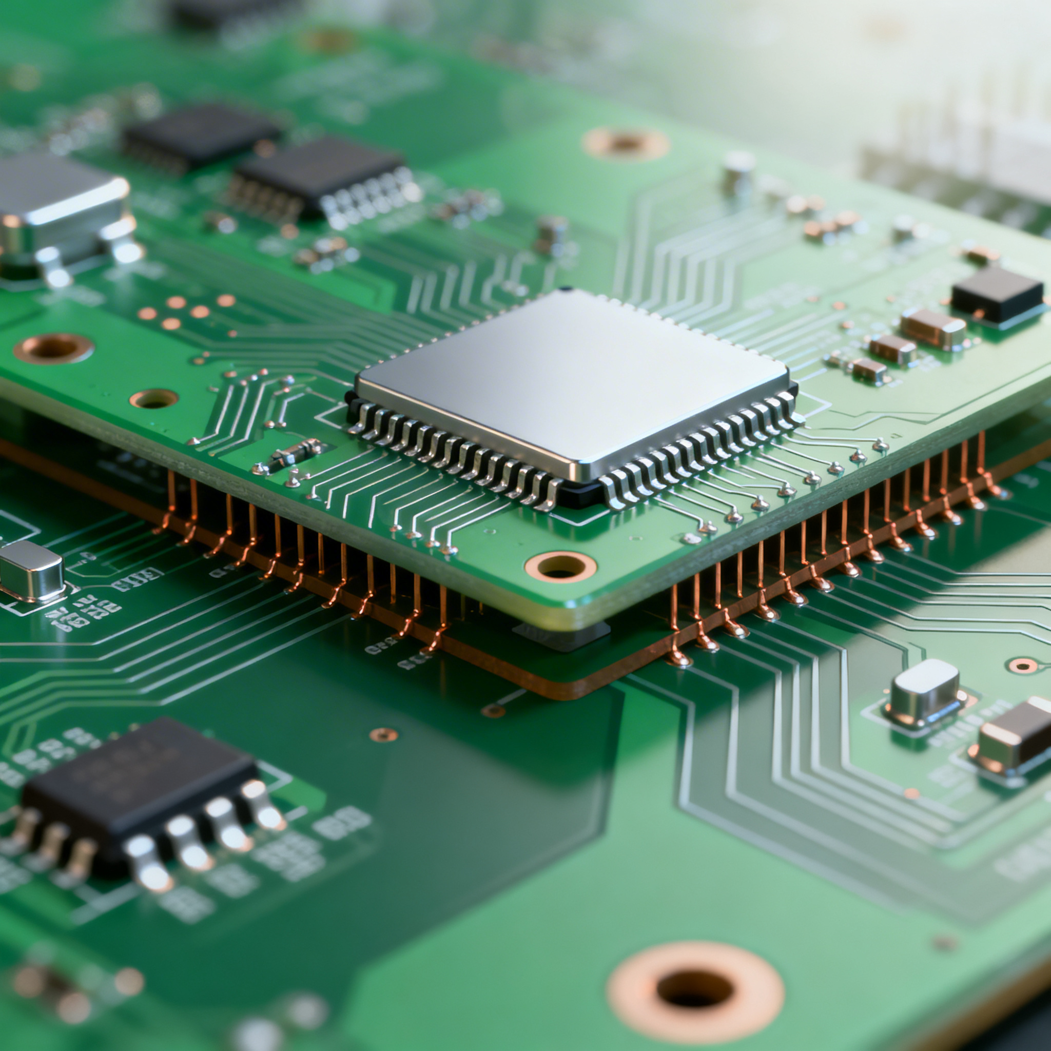
PCB assembly involves mounting various components, including ICs, onto a PCB. The process encompasses design, component selection, soldering, and testing. The architecture of a PCB is defined by its layers, traces, and the components it integrates. Key principles include signal integrity, thermal management, and power distribution. Understanding the architecture and principles allows engineers to make informed decisions, ensuring functionality while minimizing costs.
Detailed Specifications
When selecting ICs for a PCB, several specifications must be considered, including CPU speed, memory capacity, available peripherals, power requirements, and packaging. These factors determine the performance and compatibility of the IC with the intended application.
| Specification | Value | Description |
|---|---|---|
| CPU Speed | 1.5 GHz | Processing speed of the IC |
| Memory | 256 MB | Internal memory capacity |
| Peripherals | UART, SPI, I2C | Supported communication interfaces |
| Power Supply | 3.3V | Voltage required for operation |
| Package | QFP | Quad Flat Package for easy mounting |
| Temperature Range | -40°C to 85°C | Operating temperature range |
| GPIO | 32 | General-purpose I/O pins available |
| Flash Memory | 512 MB | On-chip storage for firmware |
| ADC | 10-bit | Analog-to-Digital Converter resolution |
| Interface | USB 2.0 | Universal Serial Bus support |
Key Takeaways from the Specifications
The specifications table provides critical insights into the capabilities of the IC. A CPU speed of 1.5 GHz ensures robust processing power suitable for complex applications. The inclusion of multiple peripherals like UART, SPI, and I2C allows for versatile communication options. A power supply of 3.3V is standard for low-power applications, while the QFP package facilitates easy soldering on the PCB. Understanding these specifications helps in selecting the right IC for the intended application, balancing performance with cost.
| Characteristic | Value | Description |
|---|---|---|
| Supply Voltage | 1.8V - 3.6V | Operating voltage range |
| Supply Current | 150 mA | Current consumption during operation |
| Input Voltage | 0V - 3.3V | Voltage range for input signals |
| Output Voltage | 0V - 3.3V | Voltage range for output signals |
| Clock Frequency | 50 MHz | Maximum operating clock frequency |
| Input Capacitance | 5 pF | Capacitance of input pins |
| Output Capacitance | 10 pF | Capacitance of output pins |
| Propagation Delay | 5 ns | Time delay from input to output |
| ESD Protection | 2 kV | Electrostatic discharge protection level |
| Leakage Current | 1 µA | Current leakage at high impedance state |
| I/O Voltage | 3.3V | Voltage level for I/O pins |
Practical Implications
The electrical characteristics table highlights the operational limits of the IC. A supply voltage range of 1.8V to 3.6V offers flexibility in power supply design. The current consumption of 150 mA is a crucial factor in power budgeting, especially for battery-operated devices. ESD protection of 2 kV ensures durability against electrostatic discharges. These parameters must be considered during the design phase to prevent overloading and ensure reliable performance.
| Use Case | Configuration | Advantages |
|---|---|---|
| Consumer Electronics | Standard Configuration | Cost-effective and widely compatible |
| Automotive | Enhanced ESD Protection | Reliable in harsh environments |
| Industrial Control | Extended Temperature Range | Operates in extreme conditions |
| Medical Devices | Low Power Consumption | Essential for battery longevity |
| Networking Equipment | High Throughput | Supports fast data processing |
| Wearable Devices | Compact Form Factor | Ideal for limited space applications |
Application Guidelines
The application comparison table demonstrates the versatility of the IC across various sectors. In consumer electronics, a standard configuration keeps costs low while maintaining compatibility. For automotive applications, enhanced ESD protection is crucial for reliability. Industrial control systems benefit from extended temperature ranges, allowing them to function in extreme environments. Understanding these applications helps in choosing the right configuration for specific needs, ensuring optimal performance and cost-efficiency.
Design Considerations
Designing a cost-effective PCB involves several critical considerations. Understanding the trade-offs between performance and cost is essential. Selecting components with optimal specifications for the intended application reduces unnecessary expenses. Implementing design for manufacturability (DFM) principles ensures that the PCB can be produced efficiently, reducing production costs. Proper layout and routing minimize signal integrity issues and enhance thermal management. Additionally, leveraging standard components and avoiding custom designs can significantly cut costs. Collaborating with suppliers and manufacturers during the design phase can provide insights into cost-saving opportunities, such as bulk purchasing discounts and alternative sourcing options.
Step-by-Step Implementation
Implementing a cost-effective PCB assembly process involves several steps:
- Define Requirements: Clearly outline the performance and cost objectives for the PCB.
- Select Components: Choose ICs and other components based on specifications, availability, and cost.
- Design Schematic: Create a detailed schematic that aligns with the defined requirements.
- Layout Design: Use CAD software to design the PCB layout, focusing on efficiency and manufacturability.
- Prototype Development: Build and test prototypes to validate the design and identify potential issues.
- Cost Analysis: Conduct a thorough cost analysis to identify areas for potential savings.
- Supplier Collaboration: Work with suppliers to explore cost-saving options such as bulk purchasing and alternative sourcing.
- Manufacturing Optimization: Implement DFM principles to streamline the manufacturing process and reduce costs.
Common Issues & Solutions
PCB assembly can encounter several common issues:
- Component Mismatch: Ensure all components are compatible with the design specifications to avoid assembly errors.
- Soldering Defects: Implement proper soldering techniques and quality control measures to prevent defects.
- Signal Integrity Issues: Optimize trace routing and use appropriate shielding to maintain signal integrity.
- Thermal Management: Incorporate heat sinks and thermal vias to manage heat dissipation effectively.
- Power Supply Instability: Design robust power distribution networks to maintain stable operation.
- ESD Damage: Use ESD protection components and follow anti-static handling procedures to prevent damage.
Applications & Use Cases
PCBs are integral to a wide range of applications, including consumer electronics, automotive systems, industrial control, medical devices, and networking equipment. Each application presents unique challenges and requirements, necessitating tailored design and component selection strategies. For example, automotive systems require robust ESD protection, while medical devices prioritize low power consumption. Understanding these use cases enables engineers to design PCBs that meet specific performance and cost objectives.
Selection & Sourcing Guide
For sourcing ICs and other components, visit IC Online for a comprehensive selection of products. Consider factors such as lead time, pricing, and supplier reliability when making purchasing decisions.
FAQ
- What is the most cost-effective way to reduce PCB assembly costs? Implementing DFM principles and selecting standard components are effective strategies.
- How can I ensure the quality of my PCB assembly? Adhering to IPC standards and conducting rigorous testing ensures high-quality assembly.
- What are the benefits of using standard components? Standard components are more readily available and often more cost-effective than custom parts.
- How do I balance performance and cost in my PCB design? Carefully evaluate specifications and prioritize features that align with the intended application.
- What role does thermal management play in PCB design? Effective thermal management prevents overheating and ensures reliable operation.
- How can I optimize my PCB layout for cost savings? Minimize layer count and use efficient routing to reduce production costs.
- What are the risks of using low-cost components? Low-cost components may compromise performance or reliability, necessitating thorough evaluation.
- How do I handle ESD protection in my PCB design? Use ESD protection devices and follow proper handling procedures to prevent damage.
- What is the importance of a supplier collaboration? Collaborating with suppliers can provide cost-saving insights and ensure component availability.
- How do I address signal integrity issues in my PCB? Optimize trace routing and use appropriate shielding techniques to maintain signal integrity.
Conclusion
Reducing PCB assembly costs while maintaining quality is a complex challenge that requires a strategic approach. By understanding component specifications, leveraging cost-saving design practices, and collaborating with suppliers, engineers can effectively balance performance and cost. This guide provides practical insights and strategies to help budget-conscious engineers optimize their PCB assembly processes, ensuring successful outcomes in a competitive industry.