pcba quality control measures
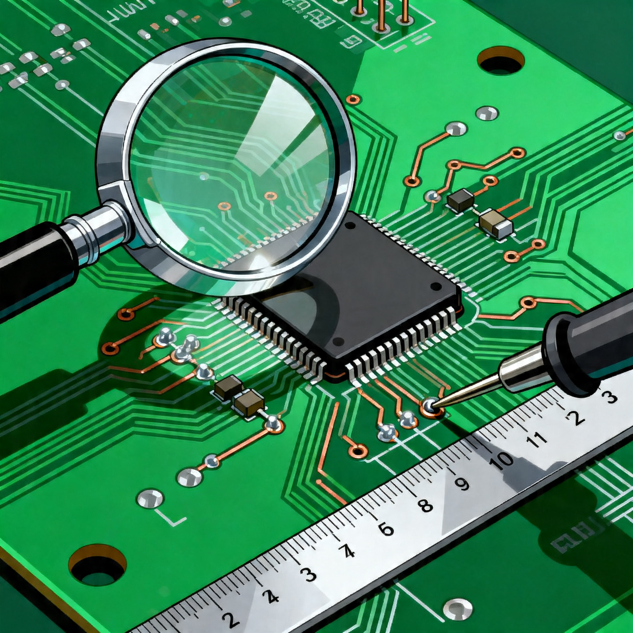
PCBA Quality Control Measures Introduction The importance of quality control in Printed Circuit Board Assembly (PCBA) cannot be overstated. As electronic devices become more complex, ensuring the reli...
Introduction
The importance of quality control in Printed Circuit Board Assembly (PCBA) cannot be overstated. As electronic devices become more complex, ensuring the reliability and functionality of PCBs is critical. Quality control measures in PCBA involve stringent adherence to design rules, stackup configurations, and material properties, which are vital for maintaining signal integrity and performance. With the advent of advanced manufacturing techniques and standards such as those outlined by the IPC, the industry has seen significant improvements in PCB design and manufacturing quality. This article delves into the essential aspects of PCBA quality control, focusing on PCB layout rules, stackup design, signal integrity, and manufacturing considerations.
Technical Overview
At the heart of PCBA quality control is the understanding of core concepts such as trace width, spacing, via sizes, and clearances. These elements are not just arbitrary numbers; they are critical parameters that determine the electrical performance and manufacturability of the board. The architecture of a PCB involves multiple layers, each with specific roles, ranging from signal layers to ground and power planes. Proper stackup design ensures that these layers work harmoniously to reduce electromagnetic interference (EMI) and crosstalk, thereby enhancing signal integrity.
Moreover, the choice of materials, such as FR-4 or Rogers, directly affects the dielectric properties of the board, influencing factors like dielectric constant and loss tangent. These properties are crucial for high-frequency applications where signal loss can be a significant issue. Understanding these principles allows engineers to design PCBs that meet both performance and reliability requirements while adhering to manufacturing constraints.
Detailed Specifications
When designing a PCB, adhering to specific design rules is crucial to ensure both performance and manufacturability. The following table outlines key PCB design rules, including trace width, spacing, via sizes, and clearances. These parameters are essential for maintaining signal integrity and ensuring the board can be manufactured without issues.
| Parameter | Minimum Value | Description |
|---|---|---|
| Trace Width | 6 mils | Minimum width for signal traces to ensure current capacity. |
| Trace Spacing | 6 mils | Minimum spacing between traces to prevent shorting and crosstalk. |
| Via Diameter | 10 mils | Diameter of vias to ensure reliable connections between layers. |
| Via Pad Size | 18 mils | Size of the pad around the via to ensure proper soldering. |
| Clearance to Edge | 10 mils | Minimum distance from traces to the edge of the PCB. |
| Power Plane Clearance | 20 mils | Clearance around power planes to prevent short circuits. |
| Drill Hole Size | 12 mils | Minimum size for drilled holes for component leads. |
| Solder Mask Clearance | 4 mils | Clearance of solder mask to avoid covering pads. |
| Annular Ring | 4 mils | Minimum width of the ring around vias and pads. |
| Silkscreen Clearance | 6 mils | Clearance between silkscreen and pads to avoid interference. |
Key Takeaways from the Specifications
The data in the table above highlights the critical parameters that influence the manufacturability and performance of a PCB. For instance, maintaining a minimum trace width and spacing is essential to handle the necessary current without overheating and to prevent electrical interference between adjacent traces. Via sizes and pad dimensions ensure robust connections between layers and components, which are vital for the board's structural integrity. These specifications are foundational for any PCB design, and deviations can lead to production issues or compromised performance.
Layer Stackup Options
Layer stackup plays a crucial role in the electrical performance of a PCB, particularly in high-speed and high-frequency applications. The arrangement of signal layers, ground planes, and power planes determines the board's impedance, crosstalk, and EMI characteristics. The following table presents different layer stackup configurations commonly used in PCB design.
| Layer Configuration | Number of Layers | Application |
|---|---|---|
| 2-Layer | 2 | Simple designs with low component density. |
| 4-Layer | 4 | Increased signal integrity with dedicated ground and power planes. |
| 6-Layer | 6 | High-speed applications with additional routing layers. |
| 8-Layer | 8 | Complex designs with multiple power domains. |
| 10-Layer | 10 | Advanced designs requiring high signal integrity and low EMI. |
| 12-Layer | 12 | Very complex designs with extensive routing requirements. |
| HDI | Varies | High-density interconnect for compact, high-performance applications. |
Practical Implications
The choice of layer stackup directly impacts the board's ability to handle complex routing and maintain signal integrity. For example, a 4-layer stackup is often sufficient for moderate complexity designs, offering good performance with dedicated ground and power planes. However, for advanced applications such as RF or high-speed digital circuits, an 8-layer or 10-layer stackup might be necessary to ensure proper impedance control and reduce EMI. HDI stackups are particularly useful in miniaturized designs where space is at a premium. Selecting the appropriate stackup is crucial for balancing performance, cost, and manufacturing complexity.
Material Properties
The choice of materials for PCB construction affects the board's electrical and thermal performance. Different materials offer varying dielectric constants and loss tangents, which are critical for applications involving high frequencies. The table below provides an overview of common PCB materials and their properties.
| Material | Dielectric Constant (Dk) | Loss Tangent (Df) |
|---|---|---|
| FR-4 | 4.5 | 0.02 |
| Rogers 4350B | 3.66 | 0.0037 |
| Rogers 4003C | 3.55 | 0.0027 |
| Isola FR408HR | 3.75 | 0.008 |
| Megtron 6 | 3.48 | 0.004 |
| Arlon 85N | 3.5 | 0.0045 |
| Nelco N4000-13 | 3.7 | 0.0055 |
| Polyimide | 3.5 | 0.0045 |
| PTFE | 2.1 | 0.001 |
Application Guidelines
The material properties outlined in the table above are critical in determining the suitability of a PCB for different applications. For instance, FR-4 is a standard material used in general-purpose applications due to its cost-effectiveness and decent electrical properties. However, for high-frequency applications, materials like Rogers 4350B or PTFE with lower dielectric constants and loss tangents are preferred to minimize signal loss and distortion. Selecting the right material involves considering the application's frequency requirements, thermal management, and cost constraints, ensuring the PCB meets the necessary performance criteria.
Design Considerations
Designing a PCB involves several considerations to ensure optimal performance and manufacturability. Key aspects include maintaining signal integrity, minimizing EMI, and ensuring thermal management. Signal integrity can be maintained by adhering to trace width and spacing rules, utilizing proper layer stackups, and selecting materials with suitable dielectric properties. EMI can be reduced by using continuous ground planes, proper shielding, and avoiding long parallel trace runs.
Thermal management is another critical consideration, especially in high-power applications. This can be achieved by using vias to transfer heat to other layers, employing thermal relief pads, and selecting materials with good thermal conductivity. Additionally, the placement of components should be carefully planned to minimize trace lengths and avoid interference. These design considerations are vital for creating a PCB that meets the desired performance, reliability, and cost objectives.
Step-by-Step Implementation
Implementing a PCB design involves several steps, each critical for ensuring the final product meets design specifications and quality standards. Here's a detailed step-by-step guide:
- Define Requirements: Begin by understanding the electrical, mechanical, and environmental requirements of the PCB.
- Schematic Design: Create a schematic diagram that outlines the circuit connections and component specifications.
- Component Selection: Choose components based on performance, availability, and cost considerations, ensuring compatibility with the design.
- PCB Layout: Utilize PCB design software to layout the components, traces, and vias, adhering to design rules for trace width, spacing, and clearances.
- Layer Stackup Design: Determine the appropriate layer stackup to balance signal integrity, EMI, and manufacturing complexity.
- Material Selection: Choose materials that meet the electrical and thermal requirements of the design, considering dielectric constant and loss tangent.
- Design Rule Check (DRC): Perform a DRC to ensure the design complies with all specified design rules and constraints.
- Prototype Fabrication: Send the design for prototype fabrication to test and validate the PCB's performance before full-scale production.
Each step is crucial for ensuring that the PCB performs as expected and meets quality standards. By following this structured approach, designers can minimize errors and optimize the PCB for its intended application.
Common Issues & Solutions
PCB design and manufacturing can present several challenges, but understanding common issues and their solutions can help mitigate problems. Here are some typical issues and how to address them:
- Signal Integrity Problems: Caused by improper trace routing or insufficient spacing. Solution: Follow design rules for trace width and spacing, and use differential pairs for high-speed signals.
- EMI Interference: Often due to poor grounding or shielding. Solution: Implement continuous ground planes and use proper shielding techniques.
- Thermal Management Issues: Result from inadequate heat dissipation. Solution: Use thermal vias, heat sinks, and select materials with good thermal conductivity.
- Manufacturing Defects: Such as shorts or opens due to design errors. Solution: Conduct thorough DRCs and work closely with manufacturers to ensure design compliance.
- Component Placement Errors: Can lead to increased trace lengths and signal delay. Solution: Optimize component placement for minimal trace lengths and reduced interference.
By anticipating these issues and implementing preventive measures, designers can improve the reliability and performance of their PCBs.
Applications & Use Cases
PCBs are integral to a wide range of applications, from consumer electronics to aerospace systems. In consumer electronics, PCBs are found in smartphones, laptops, and home appliances, where compactness and cost are critical. In automotive and aerospace applications, PCBs must withstand harsh environments and maintain high reliability, often using specialized materials and stackups for enhanced performance. Additionally, PCBs are crucial in industrial and medical devices, where precision and durability are paramount. Each application has unique requirements, influencing the design and material choices for the PCB.
Selection & Sourcing Guide
When selecting and sourcing components and materials for PCB design, consider factors such as availability, cost, and supplier reliability. Resources like IC Online offer extensive databases of components and suppliers, making it easier to find the right parts for your design. Evaluating supplier quality, lead times, and support services is also crucial for ensuring a smooth manufacturing process.
FAQ
- What is the importance of trace width in PCB design? Trace width is crucial for handling the required current and minimizing resistance, which affects signal integrity and thermal performance.
- How does layer stackup affect signal integrity? Proper layer stackup reduces crosstalk and EMI, ensuring stable signal transmission, especially in high-speed applications.
- What materials are best for high-frequency PCBs? Materials like Rogers 4350B and PTFE are preferred for their low dielectric constants and loss tangents, minimizing signal loss.
- Why is solder mask clearance important? Solder mask clearance prevents accidental bridging during soldering, ensuring reliable electrical connections.
- How can I reduce EMI in my PCB design? Use continuous ground planes, proper shielding, and avoid long parallel trace runs to minimize EMI.
- What are the consequences of poor thermal management? Inadequate thermal management can lead to overheating, component failure, and reduced lifespan of the PCB.
- How do I choose the right PCB material? Consider the application's frequency, thermal requirements, and cost constraints when selecting materials.
- What role does DRC play in PCB design? Design Rule Check ensures that the design adheres to specified rules and constraints, minimizing the risk of manufacturing defects.
- Can I use a 2-layer PCB for complex designs? While possible, a 2-layer PCB may not provide adequate signal integrity or routing options for complex designs. Consider a multi-layer stackup.
- How does component placement affect PCB performance? Optimal component placement reduces trace lengths, minimizes interference, and improves overall performance.
Conclusion
In conclusion, PCBA quality control measures are vital for ensuring the reliability and performance of electronic devices. By adhering to design rules, selecting appropriate materials, and carefully planning layer stackups, engineers can create PCBs that meet stringent quality standards. Understanding these principles and applying them effectively in the design process is crucial for success in today's competitive electronics industry.