Introduction
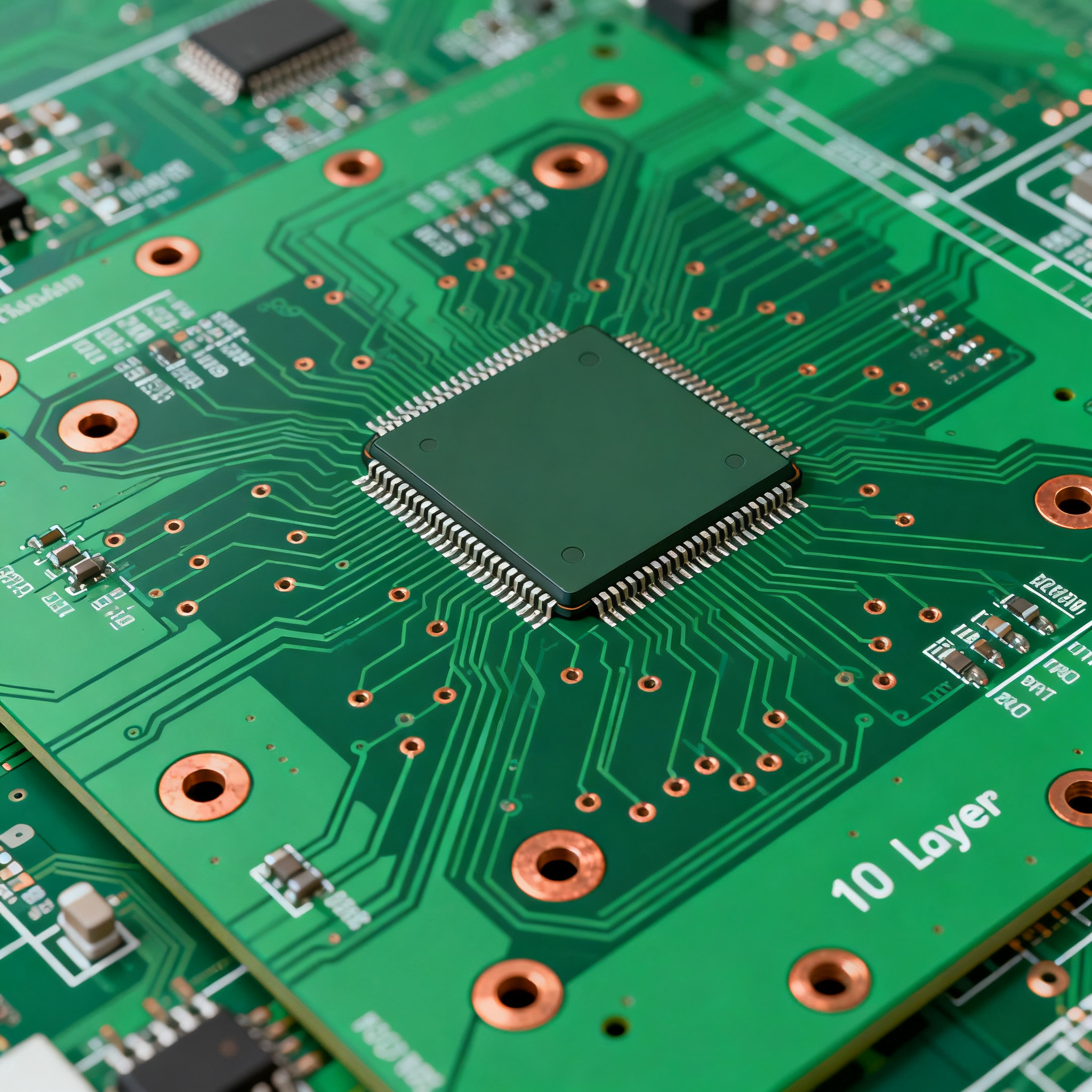
In the ever-evolving landscape of electronics, designing a high-reliability 10-layer Printed Circuit Board Assembly (PCBA) requires meticulous attention to detail and adherence to stringent design rules. The complexity of these multi-layer boards demands a comprehensive understanding of circuit topology, component calculations, performance analysis, and design trade-offs. This article delves into the essential guidelines for ensuring reliability in your 10-layer assemblies, drawing from industry standards such as IPC and leveraging resources from PCB manufacturing experts. By exploring detailed specifications, performance metrics, and practical design considerations, this guide aims to equip you with the knowledge necessary to optimize your PCBA designs for both performance and reliability.
Technical Overview
At the heart of any complex electronic device lies the PCBA, a critical component that interconnects various electronic elements. A typical 10-layer PCBA involves a sophisticated architecture where multiple layers are stacked to accommodate intricate circuit designs. The layers often include power planes, ground planes, and signal layers, each serving a distinct purpose in the overall topology. Key principles in PCBA design include signal integrity, thermal management, and electromagnetic compatibility (EMC).
Signal integrity ensures that the signals on the board maintain their quality without distortion, which is crucial for high-speed applications. Thermal management is another vital aspect, as excessive heat can lead to component failure and reduced lifespan. Proper layout and material selection play pivotal roles in dissipating heat effectively. EMC involves designing the board in a way that minimizes electromagnetic interference, ensuring the device operates correctly in its intended environment.
Understanding these core concepts is essential for designing a reliable 10-layer PCBA. By adhering to industry standards and employing best practices, engineers can create designs that not only meet performance requirements but also adhere to manufacturing constraints and cost considerations.
Detailed Specifications
When designing a 10-layer PCBA, several specifications are critical to ensure reliability and performance. These specifications include component values, layout considerations, and electrical characteristics. Understanding these parameters allows engineers to make informed decisions during the design process.
| Parameter | Value | Formula/Calculation |
| Resistor Value | 10kΩ | Ohm's Law: V=IR |
| Capacitor Value | 1µF | C=Q/V |
| Inductor Value | 10µH | L=V*(dt/dI) |
| Trace Width | 0.2 mm | IPC-2221: Current capacity |
| Dielectric Constant | 4.2 | ε_r=ε/ε_0 |
| Layer Thickness | 1.6 mm | Standard PCB thickness |
| Via Diameter | 0.3 mm | IPC-2221: Aspect ratio |
| Power Plane Voltage | 3.3V | Standard logic level |
| Ground Plane Impedance | 50Ω | Z=√(L/C) |
| Signal Rise Time | 1ns | Tr=0.35/BW |
| Isolation Resistance | 10MΩ | R_iso=V/I_leak |
Key Takeaways from the Specifications
The specifications outlined in Table 1 provide a foundation for designing a reliable 10-layer PCBA. Component values such as resistors, capacitors, and inductors are determined based on the expected electrical performance and environmental conditions. The trace width and via diameter are critical for ensuring adequate current carrying capacity and mechanical stability, respectively. The dielectric constant and layer thickness influence the board's electrical characteristics, impacting signal integrity and impedance control. Understanding these parameters allows engineers to optimize the design for both performance and manufacturability, ensuring the final product meets the desired specifications.
| Performance Metric | Value | Significance |
| Gain | 10 dB | Amplification level |
| Bandwidth | 2 GHz | Frequency range |
| Signal-to-Noise Ratio (SNR) | 60 dB | Signal clarity |
| Power Consumption | 5 W | Energy efficiency |
| Thermal Resistance | 1.5 °C/W | Heat dissipation |
| Crosstalk | -40 dB | Signal interference |
| Return Loss | -20 dB | Signal reflection |
| Voltage Standing Wave Ratio (VSWR) | 1.2:1 | Impedance matching |
| Phase Margin | 45° | Stability |
| Noise Figure | 3 dB | Signal quality |
Practical Implications
The performance metrics in Table 2 are crucial for evaluating the effectiveness of a 10-layer PCBA. Gain and bandwidth define the amplification and frequency range of the circuit, impacting its suitability for various applications. A high signal-to-noise ratio ensures clear signal transmission, while low power consumption indicates energy efficiency. Thermal resistance and crosstalk are critical for thermal management and minimizing signal interference. Understanding these metrics allows engineers to assess the board's performance and make necessary adjustments to enhance reliability and functionality.
| Configuration | Pros | Cons |
| Thick Copper Layers | High current capacity | Increased cost |
| Microvias | Space-efficient | Complex manufacturing |
| Embedded Components | Reduced footprint | Repair challenges |
| Blind/Buried Vias | Signal integrity | Higher cost |
| High-Density Interconnect (HDI) | Compact design | Expensive |
| Flexible PCB | Versatility | Lower durability |
| FR-4 Material | Cost-effective | Limited high-frequency performance |
| Metal Core PCB | Excellent thermal management | Heavier |
Application Guidelines
The design trade-offs highlighted in Table 3 provide insights into different configurations and their implications. Thick copper layers offer high current capacity but at an increased cost, while microvias allow for space-efficient designs but require complex manufacturing processes. Embedded components reduce the board's footprint but pose challenges in repairability. Understanding these trade-offs helps in selecting the right configuration based on the specific requirements of the application, balancing performance, cost, and manufacturability.
Design Considerations
When designing a 10-layer PCBA, several practical guidelines must be followed to ensure reliability and performance. Key considerations include:
- Layer Stackup: Carefully plan the layer stackup to optimize signal routing, power distribution, and grounding. Ensure that power and ground planes are adjacent to signal layers to minimize impedance and enhance signal integrity.
- Thermal Management: Incorporate thermal vias and heat sinks to dissipate heat effectively. Use materials with high thermal conductivity and design the board layout to facilitate airflow.
- EMC Compliance: Design the board to minimize electromagnetic interference. Use shielding techniques, such as ground planes and ferrite beads, and ensure proper spacing between traces.
- Signal Integrity: Pay attention to trace lengths, impedance matching, and termination techniques. Use differential signaling for high-speed signals to reduce noise and crosstalk.
- Design for Manufacturability: Collaborate with your manufacturer to ensure the design meets their capabilities. Consider factors such as minimum trace width, via sizes, and panelization requirements.
By adhering to these guidelines, engineers can create designs that are not only robust and reliable but also optimized for performance and manufacturability.
Step-by-Step Implementation
Designing a 10-layer PCBA involves a series of detailed steps, each critical to the final product's success. Here's a step-by-step guide:
- Define Requirements: Begin by defining the functional and performance requirements of your PCBA. Consider factors such as operating environment, electrical specifications, and mechanical constraints.
- Choose Materials: Select appropriate materials based on thermal, mechanical, and electrical properties. FR-4 is a common choice, but alternative materials may be needed for high-frequency applications.
- Design Layer Stackup: Plan the layer stackup to optimize routing and signal integrity. Ensure that critical signals have a clear path and are adequately shielded by ground planes.
- Schematic Design: Create a detailed schematic that includes all components, connections, and electrical characteristics. Validate the design through simulations to ensure it meets the specified requirements.
- PCB Layout: Translate the schematic into a physical layout, placing components strategically to minimize trace lengths and enhance thermal management. Pay attention to routing, via placement, and layer transitions.
- Perform DFM Analysis: Conduct a Design for Manufacturability (DFM) analysis to ensure the design meets manufacturing constraints. Collaborate with your manufacturer to address any potential issues.
- Prototype and Test: Fabricate a prototype and conduct thorough testing to validate the design. Assess performance metrics such as gain, bandwidth, and thermal resistance, and make necessary adjustments.
- Finalize Design: Incorporate feedback from testing and finalize the design. Prepare detailed documentation, including assembly instructions and testing procedures, to facilitate production.
Following these steps ensures a systematic approach to designing a 10-layer PCBA, resulting in a reliable and high-performance product.
Common Issues & Solutions
Designing a 10-layer PCBA can present several challenges. Here are common issues and their solutions:
- Signal Integrity Problems: These can arise from improper routing or impedance mismatches. Solution: Use controlled impedance traces and differential signaling for high-speed signals.
- Thermal Management Challenges: Excessive heat can lead to component failure. Solution: Incorporate thermal vias and heat sinks, and use materials with high thermal conductivity.
- EMC Non-compliance: Electromagnetic interference can disrupt circuit operation. Solution: Implement shielding techniques and ensure proper grounding and spacing between traces.
- Manufacturing Constraints: Issues such as trace width violations can occur during fabrication. Solution: Collaborate with manufacturers early in the design process to ensure compliance with their capabilities.
- Component Placement Issues: Poor placement can affect performance and manufacturability. Solution: Use automated tools for optimal component placement and ensure clear routing paths.
- Testing Difficulties: Complex designs can be challenging to test. Solution: Design with testability in mind, incorporating test points and using automated testing procedures.
By addressing these issues proactively, engineers can enhance the reliability and performance of their 10-layer PCBA designs.
Applications & Use Cases
10-layer PCBAs find applications in a variety of industries due to their ability to support complex circuits and high-density designs. Some real-world examples include:
- Telecommunications: Used in high-speed communication devices and infrastructure, where signal integrity and bandwidth are critical.
- Automotive Electronics: Employed in advanced driver-assistance systems (ADAS) and infotainment systems, requiring robust performance and reliability.
- Aerospace and Defense: Utilized in avionics and military electronics for their durability and ability to withstand harsh environments.
- Medical Devices: Integrated into diagnostic equipment and wearable devices, where precision and reliability are paramount.
These applications demonstrate the versatility and importance of 10-layer PCBAs in modern electronics, highlighting their role in enabling advanced technologies.
Selection & Sourcing Guide
When selecting components and materials for your 10-layer PCBA, it's essential to consider factors such as performance, cost, and availability. Utilize resources like
IC Online to source components and ensure compatibility with your design. Collaborate with suppliers to secure reliable components and maintain a consistent supply chain, reducing the risk of delays and ensuring the timely production of your assemblies.
FAQ
Here are some frequently asked questions about 10-layer PCBA design:
- What are the benefits of a 10-layer PCBA? 10-layer PCBAs offer increased routing space, improved signal integrity, and enhanced thermal management, making them suitable for complex and high-density designs.
- How do I ensure signal integrity in a multi-layer board? Use controlled impedance traces, differential signaling, and proper grounding techniques to maintain signal integrity.
- What materials are best for high-frequency applications? Materials with low dielectric loss, such as Rogers or Teflon-based substrates, are ideal for high-frequency applications.
- How can I manage heat in a 10-layer PCBA? Incorporate thermal vias, heat sinks, and materials with high thermal conductivity to dissipate heat effectively.
- What is the role of a ground plane in a multi-layer board? Ground planes provide a reference point for signals, reduce electromagnetic interference, and improve signal integrity.
- How do I address EMC issues in my design? Implement shielding techniques, ensure proper grounding, and maintain adequate spacing between traces to minimize electromagnetic interference.
- What is the significance of a DFM analysis? Design for Manufacturability (DFM) analysis ensures the design meets manufacturing constraints, reducing the risk of fabrication issues.
- How do I select the right components for my design? Consider factors such as performance, cost, availability, and compatibility with your design requirements.
- What are the challenges of using microvias? Microvias offer space efficiency but require complex manufacturing processes, potentially increasing costs.
- How can I ensure the reliability of my 10-layer PCBA? Follow industry standards, adhere to design guidelines, and conduct thorough testing to ensure reliability and performance.
Conclusion
Designing a reliable 10-layer PCBA requires a comprehensive understanding of circuit topology, performance metrics, and design trade-offs. By adhering to industry standards and employing best practices, engineers can create designs that meet stringent performance requirements while remaining cost-effective and manufacturable. This guide provides a detailed overview of the essential guidelines for designing high-reliability 10-layer assemblies, equipping you with the knowledge needed to succeed in the complex world of electronics design.