PCB vs. PCBA: Key Differences Every Engineer Should Know for Optimized Production
Introduction In today’s rapidly evolving electronics industry, the distinction between Printed Circuit Boards (PCBs) and Printed Circuit Board Assemblies (PCBAs) is crucial for engineers aiming to opt...
Introduction
In today’s rapidly evolving electronics industry, the distinction between Printed Circuit Boards (PCBs) and Printed Circuit Board Assemblies (PCBAs) is crucial for engineers aiming to optimize production processes. PCBs serve as the foundational framework upon which electronic components are mounted, while PCBAs represent the completed assembly of these components. Understanding the differences and nuances between PCB and PCBA is vital for ensuring design integrity, manufacturing efficiency, and overall product success. This article delves into the key differences, focusing on PCB design rules, layer stackup options, material properties, and their implications in the manufacturing process.
Technical Overview
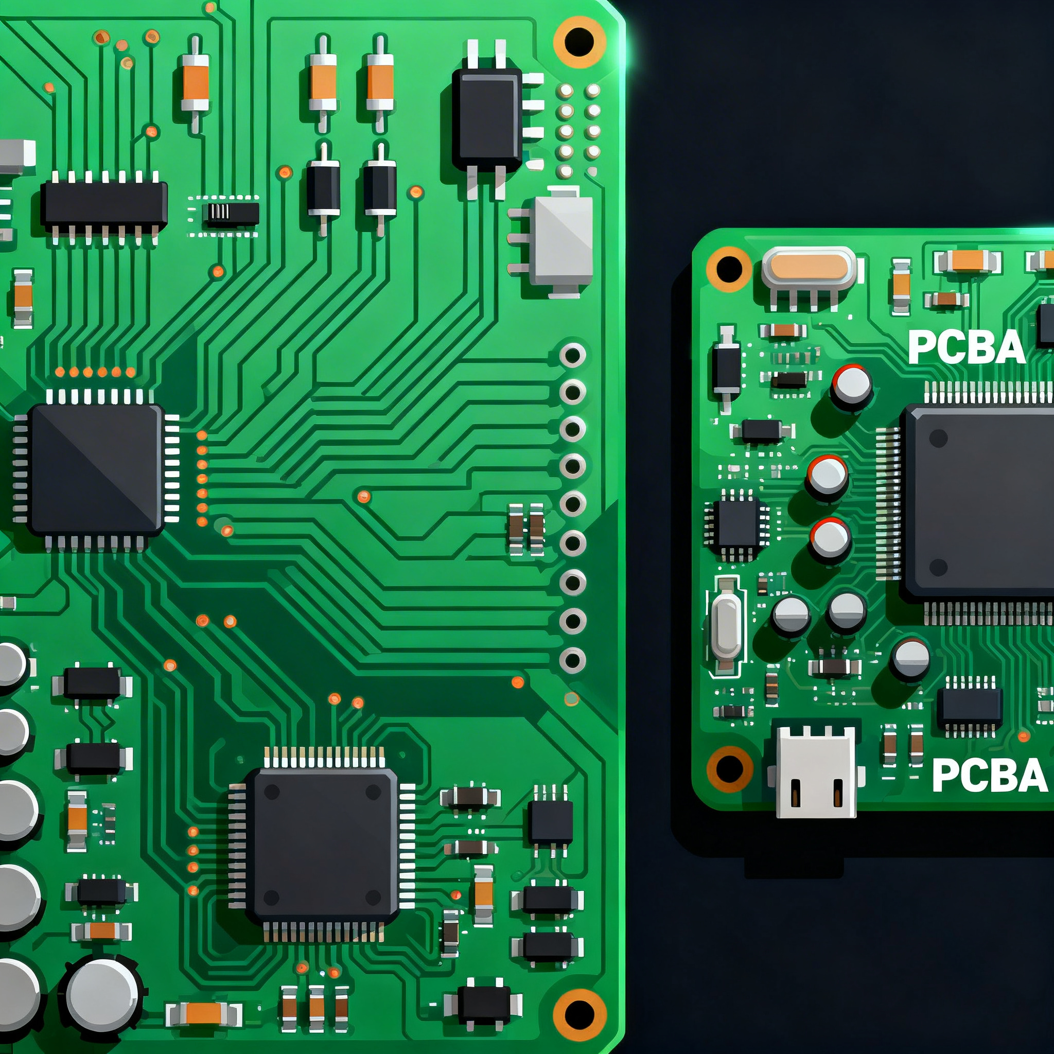
PCBs and PCBAs form the backbone of modern electronic devices. A PCB is essentially a bare board that provides the physical platform for electrical connections between components. It includes layers of copper and other materials laminated together. The design of a PCB involves meticulous attention to layout rules, stackup design, and signal integrity to ensure reliability and performance. On the other hand, a PCBA is the end product of mounting electronic components onto a PCB. This process involves soldering, inspection, and testing to ensure functionality. The architecture of a PCB includes various layers and materials that affect its electrical properties and performance. Key principles such as trace width, spacing, via sizes, and clearances are foundational to PCB design, while considerations for signal integrity and thermal management are essential for PCBA performance.
Detailed Specifications
Understanding the detailed specifications of PCB design is crucial for achieving optimal performance and manufacturability. The following table outlines essential PCB design rules, which serve as the guidelines for creating robust and reliable circuit boards.
| Design Rule | Specification | Importance |
|---|---|---|
| Trace Width | 0.15 mm minimum | Ensures current handling capability |
| Trace Spacing | 0.15 mm minimum | Prevents short circuits |
| Via Size | 0.3 mm minimum | Facilitates layer transitions |
| Pad Size | 0.5 mm minimum | Supports component mounting |
| Clearance | 0.2 mm minimum | Avoids electrical interference |
| Solder Mask Clearance | 0.1 mm minimum | Prevents solder bridging |
| Drill Hole Size | 0.3 mm minimum | Accommodates component leads |
| Annular Ring | 0.1 mm minimum | Ensures robust connections |
| Aspect Ratio | 6:1 maximum | Maintains via integrity |
| Impedance Control | ±10% tolerance | Ensures signal integrity |
Key Takeaways from the Specifications
The PCB design rules outlined in the table are fundamental to ensuring the electrical and mechanical reliability of a circuit board. Proper trace width and spacing are critical for preventing overheating and short circuits, while adequate via and pad sizes ensure reliable connections and component mounting. Clearances and solder mask specifications help prevent solder bridging and electrical interference. Drill hole sizes and annular rings are essential for accommodating component leads and ensuring robust connections. Maintaining the aspect ratio within limits preserves via integrity, and strict impedance control is necessary for preserving signal integrity, especially in high-frequency applications.
| Layer Configuration | Usage | Benefits |
|---|---|---|
| 2-Layer | Simple designs | Cost-effective |
| 4-Layer | Moderate complexity | Improved signal integrity |
| 6-Layer | High-speed circuits | Enhanced EMI control |
| 8-Layer | Advanced designs | Superior power distribution |
| 10-Layer | Complex RF applications | Optimal signal routing |
| 12-Layer | High-density boards | Maximum component integration |
| 14-Layer | Ultra-complex systems | Ultimate performance |
Practical Implications
The choice of layer stackup configuration is a significant consideration in PCB design, influencing both performance and cost. Simpler 2-layer boards are cost-effective for basic applications, while 4-layer boards provide improved signal integrity for moderate complexity designs. As complexity increases, 6-layer and 8-layer boards offer enhanced EMI control and power distribution. For high-speed and RF applications, 10-layer and beyond configurations are essential for optimal signal routing and component integration. The choice of stackup affects manufacturing complexity, cost, and the board's ability to handle high-speed signals and power distribution efficiently.
| Material | Dielectric Constant (Dk) | Loss Tangent (Df) |
|---|---|---|
| FR-4 | 4.5 | 0.02 |
| Rogers 4350B | 3.66 | 0.0037 |
| Rogers 4003C | 3.38 | 0.0027 |
| Isola 370HR | 4.04 | 0.019 |
| Nelco N4000-13 | 3.9 | 0.016 |
| Polyimide | 4.2 | 0.015 |
| PTFE | 2.1 | 0.001 |
| BT Epoxy | 4.0 | 0.016 |
| Ceramic | 6.5 | 0.002 |
Application Guidelines
The choice of material significantly impacts a PCB's electrical performance and suitability for different applications. FR-4 is a versatile and cost-effective material suitable for general-purpose applications, whereas materials like Rogers 4350B and 4003C are preferred for high-frequency and RF applications due to their lower dielectric constants and loss tangents. Isola 370HR and Nelco N4000-13 are excellent for high-reliability applications, offering balanced performance. Polyimide is ideal for high-temperature environments, while PTFE and ceramic materials are used in specialized applications requiring exceptional dielectric properties. Selecting the right material involves balancing performance requirements with cost considerations and environmental factors.
Design Considerations
When designing a PCB, engineers must consider several factors to ensure optimal performance and manufacturability. Key design considerations include trace routing, layer stackup, and material selection, all of which affect the board's electrical and thermal performance. Additionally, engineers must account for signal integrity, power distribution, and thermal management to prevent issues such as crosstalk, voltage drop, and overheating. Design for manufacturability (DFM) principles should also be applied to streamline production and reduce costs. By adhering to industry standards, such as those provided by IPC, and leveraging advanced design tools, engineers can create PCBs that meet performance requirements while minimizing production challenges.
Step-by-Step Implementation
The following steps outline the process of designing and manufacturing a PCB:
- Define Requirements: Identify the electrical, mechanical, and environmental requirements for the PCB.
- Choose Materials: Select appropriate materials based on dielectric properties, thermal performance, and cost.
- Design Schematic: Create a schematic diagram to define electrical connections and component placement.
- Layout Design: Implement design rules for trace routing, layer stackup, and component placement using CAD software.
- Simulate Performance: Use simulation tools to analyze signal integrity, thermal performance, and power distribution.
- Generate Gerber Files: Export the design to Gerber format for manufacturing.
- Prototype and Test: Manufacture a prototype board and conduct testing to verify functionality and performance.
- Iterate and Finalize: Make necessary design adjustments based on prototype testing and finalize the design for mass production.
Common Issues & Solutions
During PCB design and manufacturing, engineers often encounter several common issues:
- Signal Integrity Problems: Use controlled impedance routing and proper termination techniques to mitigate signal integrity issues.
- Thermal Management Challenges: Implement thermal vias, heat sinks, and proper component placement to manage heat dissipation.
- Manufacturing Defects: Apply design for manufacturability (DFM) principles to minimize defects such as solder bridging and misalignment.
- Crosstalk: Maintain adequate spacing between traces and use ground planes to reduce crosstalk.
- Power Integrity Issues: Ensure adequate power distribution network design to prevent voltage drops and ensure stable power supply.
- Component Placement Errors: Use automated design tools to optimize component placement and prevent assembly errors.
Applications & Use Cases
PCBs find applications across a wide range of industries, including consumer electronics, automotive, aerospace, and telecommunications. Consumer electronics such as smartphones, laptops, and wearables rely on compact and efficient PCB designs for enhanced functionality. In the automotive industry, PCBs are used in infotainment systems, engine control units, and advanced driver assistance systems (ADAS). Aerospace applications demand high-reliability PCBs for avionics and communication systems. Telecommunications infrastructure relies on PCBs for network routers, switches, and base stations, where signal integrity and reliability are paramount.
Selection & Sourcing Guide
When selecting and sourcing PCBs and PCBAs, engineers should consider factors such as material properties, manufacturing capabilities, and turnaround times. Partnering with reputable manufacturers like IC Online ensures access to high-quality components and services. It is essential to evaluate a manufacturer's compliance with industry standards, quality assurance processes, and ability to meet project-specific requirements.
FAQ
- What is the difference between a PCB and a PCBA?
A PCB is a bare board, while a PCBA is a PCB with mounted electronic components. - Why is layer stackup important in PCB design?
Layer stackup affects signal integrity, power distribution, and overall board performance. - How do I choose the right material for my PCB?
Consider electrical properties, thermal performance, and cost when selecting materials. - What are the common manufacturing defects in PCB assembly?
Common defects include solder bridging, misalignment, and insufficient solder joints. - How can I improve signal integrity in my PCB design?
Use controlled impedance routing, proper termination, and maintain adequate trace spacing. - What are the benefits of using simulation tools in PCB design?
Simulation tools help analyze and optimize signal integrity, thermal performance, and power distribution. - How does DFM help in PCB manufacturing?
DFM principles streamline production, reduce costs, and minimize manufacturing defects. - What factors should I consider when sourcing PCBAs?
Consider material quality, manufacturing capabilities, and compliance with industry standards. - How do I ensure the reliability of my PCB design?
Adhere to design rules, use quality materials, and conduct thorough testing and validation. - What is the role of IPC standards in PCB design?
IPC standards provide guidelines for design, assembly, and quality inspection to ensure reliability and performance.
Conclusion
Understanding the differences between PCBs and PCBAs is essential for optimizing production and ensuring the success of electronic products. By adhering to design rules, selecting appropriate materials, and considering layer stackup options, engineers can create reliable and efficient circuit boards. Partnering with reputable manufacturers and leveraging industry standards further enhances the quality and performance of PCBAs. As technology continues to advance, staying informed about best practices and emerging trends in PCB design and manufacturing will remain crucial for engineers in the field.