PCB vs PCBA: Key Differences Every Engineer Should Know Before Starting a Project
PCB vs PCBA: Key Differences Every Engineer Should Know Introduction In the electronics industry, understanding the nuances between Printed Circuit Boards (PCBs) and Printed Circuit Board Assemblies (...
Introduction
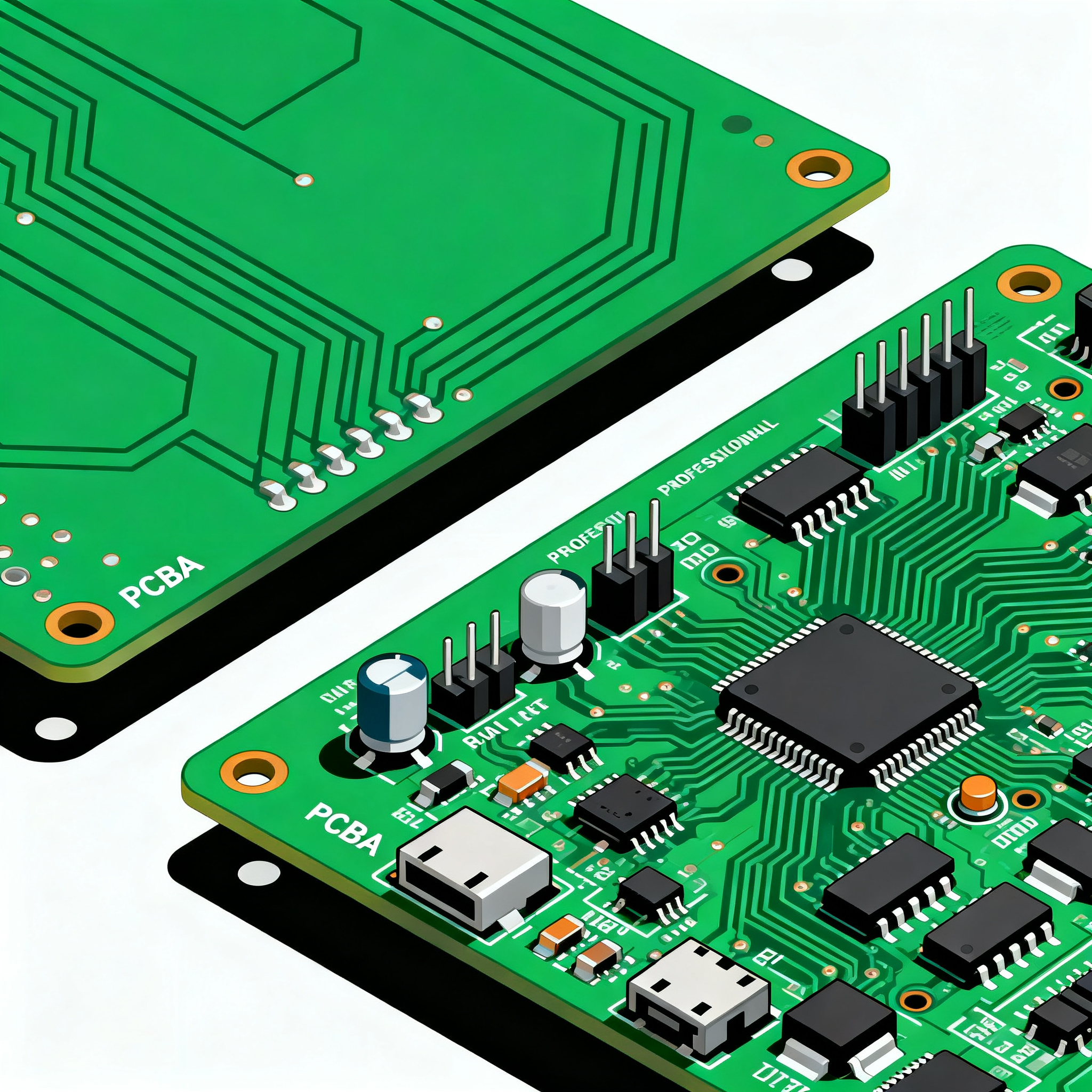
In the electronics industry, understanding the nuances between Printed Circuit Boards (PCBs) and Printed Circuit Board Assemblies (PCBAs) is crucial for engineers embarking on any design or manufacturing project. PCBs serve as the foundational platform for electronic components, while PCBAs are the finished products that include all the necessary components soldered onto the PCB. This distinction is vital as it affects design decisions, cost implications, and manufacturing processes. With advancements in technology and increasing complexity in electronic devices, engineers must be well-versed in PCB layout rules, stackup design, signal integrity, and manufacturing considerations to ensure successful project outcomes.
Technical Overview
The core concepts of PCBs and PCBAs revolve around their architecture and function within electronic devices. A PCB is essentially a board made of non-conductive material with conductive pathways etched onto it. These pathways facilitate electrical connections between various components. In contrast, a PCBA is a complete assembly that includes the PCB and all its components, such as resistors, capacitors, and integrated circuits, soldered into place. The design and manufacturing processes of PCBs and PCBAs are guided by standards such as IPC-2221, which provides general design principles, and IPC-A-610, which outlines acceptance criteria for electronic assemblies.
Engineers must consider several factors when designing PCBs, including trace width, spacing, via sizes, and clearances, to ensure signal integrity and reliable performance. Additionally, the layer stackup and material selection play a critical role in the board's overall functionality. Understanding these technical aspects is essential for optimizing design, reducing errors, and minimizing costs during manufacturing and assembly.
Detailed Specifications
When embarking on a PCB design project, it is imperative to consider specific design rules that govern the layout and functionality of the board. These specifications help maintain signal integrity, ensure manufacturability, and comply with industry standards. Key specifications include trace width, trace spacing, via sizes, and clearances. Each parameter must be carefully calculated to prevent issues such as signal crosstalk, impedance mismatches, and physical interference between components.
| Design Parameter | Value | Description |
|---|---|---|
| Minimum Trace Width | 6 mil | Width of the conductive trace |
| Minimum Trace Spacing | 6 mil | Distance between adjacent traces |
| Via Diameter | 0.3 mm | Diameter of the drilled hole |
| Pad Size | 0.6 mm | Size of the copper pad around the via |
| Clearance to Edge | 0.5 mm | Distance from trace to board edge |
| Minimum Annular Ring | 0.1 mm | Ring of copper around the via |
| Controlled Impedance | 50 ohms | Characteristic impedance for RF signals |
| Silkscreen Clearance | 0.15 mm | Distance from silkscreen to copper |
| Minimum Drill Size | 0.2 mm | Smallest hole size that can be drilled |
| Aspect Ratio | 10:1 | Ratio of board thickness to hole diameter |
Key Takeaways from the Specifications
The specifications outlined in Table 1 are critical for ensuring the reliability and performance of a PCB. For instance, maintaining a minimum trace width of 6 mil and spacing of 6 mil helps prevent electrical shorts and signal interference. The via diameter and pad size influence the board's mechanical strength and electrical connectivity. Controlled impedance is particularly important for high-frequency applications, ensuring that signal integrity is maintained across the board. These parameters must be tailored to suit the specific requirements of the project, taking into account factors such as signal speed, board size, and component density.
| Layer Configuration | Number of Layers | Typical Applications |
|---|---|---|
| Single Layer | 1 | Simple circuits, low-cost applications |
| Double Layer | 2 | Consumer electronics, moderate complexity |
| Four Layer | 4 | Multimedia devices, moderate signal integrity |
| Six Layer | 6 | High-speed digital circuits, improved EMI performance |
| Eight Layer | 8 | Advanced computing, high signal integrity |
| Ten Layer | 10 | Telecommunications, complex routing |
| Twelve Layer | 12 | Military and aerospace, critical applications |
Practical Implications
The choice of layer stackup significantly impacts the PCB's performance and cost. Single-layer boards are cost-effective but limited in complexity, making them suitable for simple applications. As the number of layers increases, so does the board's capability to handle complex circuits and maintain signal integrity. For instance, a six-layer board is ideal for high-speed digital circuits due to its ability to separate power and signal layers, reducing electromagnetic interference (EMI). Engineers must balance the need for additional layers with the associated increase in manufacturing costs and complexity.
| Material Type | Dielectric Constant (Dk) | Loss Tangent (Df) |
|---|---|---|
| FR-4 | 4.5 | 0.02 |
| Rogers 4350B | 3.66 | 0.0037 |
| Rogers 4003C | 3.55 | 0.0027 |
| PTFE (Teflon) | 2.1 | 0.001 |
| Polyimide | 3.5 | 0.004 |
| Ceramic | 9.8 | 0.0015 |
| FR-1 | 4.7 | 0.025 |
| FR-2 | 4.8 | 0.035 |
Application Guidelines
Selecting the right material for a PCB is crucial for achieving the desired electrical performance. FR-4 is a commonly used material due to its balance of electrical properties and cost-effectiveness. However, for applications requiring lower dielectric losses, materials like Rogers 4350B and PTFE are preferred due to their lower loss tangent values. High-frequency applications often use materials with lower dielectric constants, such as PTFE, to minimize signal attenuation. Engineers must consider the operational environment, frequency requirements, and cost constraints when selecting materials to ensure optimal performance and reliability.
Design Considerations
Designing a PCB involves several critical considerations to ensure functionality and manufacturability. Engineers must adhere to industry standards such as IPC-2221 for general design principles and IPC-A-610 for assembly acceptance criteria. Key design considerations include:
- Trace Width and Spacing: Ensuring adequate width and spacing to prevent shorts and maintain signal integrity.
- Layer Stackup: Choosing the right number of layers to balance performance and cost.
- Material Selection: Selecting materials based on dielectric properties and loss tangent for specific applications.
- Thermal Management: Implementing strategies to dissipate heat effectively, such as using thermal vias and heat sinks.
- Signal Integrity: Designing for controlled impedance and minimizing EMI through proper routing and grounding techniques.
- Manufacturing Constraints: Considering the limitations of fabrication processes, such as minimum drill sizes and aspect ratios.
By addressing these considerations during the design phase, engineers can optimize the PCB for performance, reliability, and cost-efficiency.
Step-by-Step Implementation
Implementing a successful PCB design requires a structured approach. Here are the steps to follow:
- Define Requirements: Clearly outline the project specifications, including electrical, mechanical, and environmental requirements.
- Schematic Design: Create a detailed schematic diagram that represents the electrical connections between components.
- Component Selection: Choose components based on availability, cost, and performance criteria.
- PCB Layout: Design the PCB layout, considering trace width, spacing, and layer stackup to ensure signal integrity.
- Simulation and Validation: Use simulation tools to validate the design and identify potential issues, such as signal integrity problems.
- Prototype Fabrication: Manufacture a prototype to test the design and make necessary adjustments.
- Testing and Debugging: Conduct thorough testing to identify and resolve any design flaws or performance issues.
- Final Production: Once validated, proceed with full-scale production, ensuring compliance with industry standards.
Following these steps ensures a systematic approach to PCB design, reducing the risk of errors and improving the overall quality of the final product.
Common Issues & Solutions
Designing and manufacturing PCBs can present various challenges. Here are some common issues and their solutions:
- Signal Crosstalk: Increase trace spacing and use differential pairs to minimize interference between signals.
- Thermal Management: Use thermal vias and copper pours to enhance heat dissipation and prevent component overheating.
- Impedance Mismatch: Implement controlled impedance routing and use appropriate materials to maintain signal integrity.
- Manufacturing Defects: Adhere to design for manufacturability (DFM) guidelines to minimize defects during production.
- Component Placement: Optimize component placement to reduce trace lengths and improve signal integrity.
- Power Integrity: Use decoupling capacitors and proper grounding techniques to maintain stable power distribution.
By addressing these issues proactively, engineers can enhance the reliability and performance of their PCB designs.
Applications & Use Cases
PCBs and PCBAs are integral to a wide range of applications across various industries. Some real-world examples include:
- Consumer Electronics: Smartphones, tablets, and wearable devices rely on compact and efficient PCB designs.
- Automotive: Advanced driver-assistance systems (ADAS) and infotainment systems use PCBs for complex circuitry.
- Telecommunications: High-frequency PCBs are essential for network infrastructure and communication devices.
- Medical Devices: PCBs are used in diagnostic equipment and wearable health monitors.
- Aerospace and Defense: Reliable and high-performance PCBs are critical for avionics and military applications.
These examples highlight the versatility and importance of PCBs and PCBAs in modern technology.
Selection & Sourcing Guide
Selecting and sourcing components for PCBs involves careful consideration of various factors, including availability, cost, and performance. Engineers can use resources like IC Online to find and compare components from multiple suppliers. Key considerations include:
- Price and Budget: Evaluate cost-effective options without compromising quality.
- Lead Time: Consider suppliers with short lead times to meet project deadlines.
- Technical Specifications: Ensure components meet the required electrical and mechanical specifications.
- Supplier Reputation: Choose reputable suppliers with a track record of reliability and quality.
By following these guidelines, engineers can effectively source components and materials for their PCB projects.
FAQ
- What is the difference between PCB and PCBA? PCB refers to the bare board, while PCBA refers to the board with components assembled.
- Why is trace width important? Trace width affects current-carrying capacity and signal integrity.
- What are the advantages of multi-layer PCBs? Multi-layer PCBs offer improved signal integrity and reduced EMI.
- How do you manage thermal issues in PCBs? Use thermal vias, heat sinks, and copper pours to enhance heat dissipation.
- What materials are commonly used for high-frequency PCBs? Materials like Rogers and PTFE are preferred for their low dielectric losses.
- How do you ensure signal integrity in PCB design? Implement controlled impedance routing and proper grounding techniques.
- What are the common manufacturing defects in PCBs? Common defects include solder bridges, open circuits, and misaligned components.
- How can I reduce EMI in my PCB design? Use proper shielding, grounding, and layer stackup to minimize EMI.
- What is the role of IPC standards in PCB design? IPC standards provide guidelines for design, assembly, and quality inspection.
- How do you select the right components for a PCB? Consider factors like availability, cost, technical specifications, and supplier reputation.
Conclusion
Understanding the differences between PCBs and PCBAs, along with the technical specifications and design considerations, is crucial for engineers to successfully execute electronic projects. By adhering to industry standards, selecting appropriate materials, and following a structured design process, engineers can ensure reliable, high-performance, and cost-effective PCB designs. This knowledge is essential for navigating the complexities of modern electronics and achieving successful project outcomes.