PCB vs PCBA: A Detailed Comparison for Engineers Who Demand Precision
PCB vs PCBA: A Detailed Comparison for Engineers Who Demand Precision Introduction In the realm of electronics engineering, understanding the distinctions between Printed Circuit Boards (PCBs) and Pri...
Introduction
In the realm of electronics engineering, understanding the distinctions between Printed Circuit Boards (PCBs) and Printed Circuit Board Assemblies (PCBAs) is crucial. These components form the backbone of modern electronic devices, influencing both functionality and reliability. Engineers who prioritize precision must delve into the specifications, performance metrics, and applications of PCBs and PCBAs to ensure optimal design and manufacturing outcomes. This detailed comparison aims to equip engineers with the knowledge needed to make informed decisions in their projects.
Technical Overview
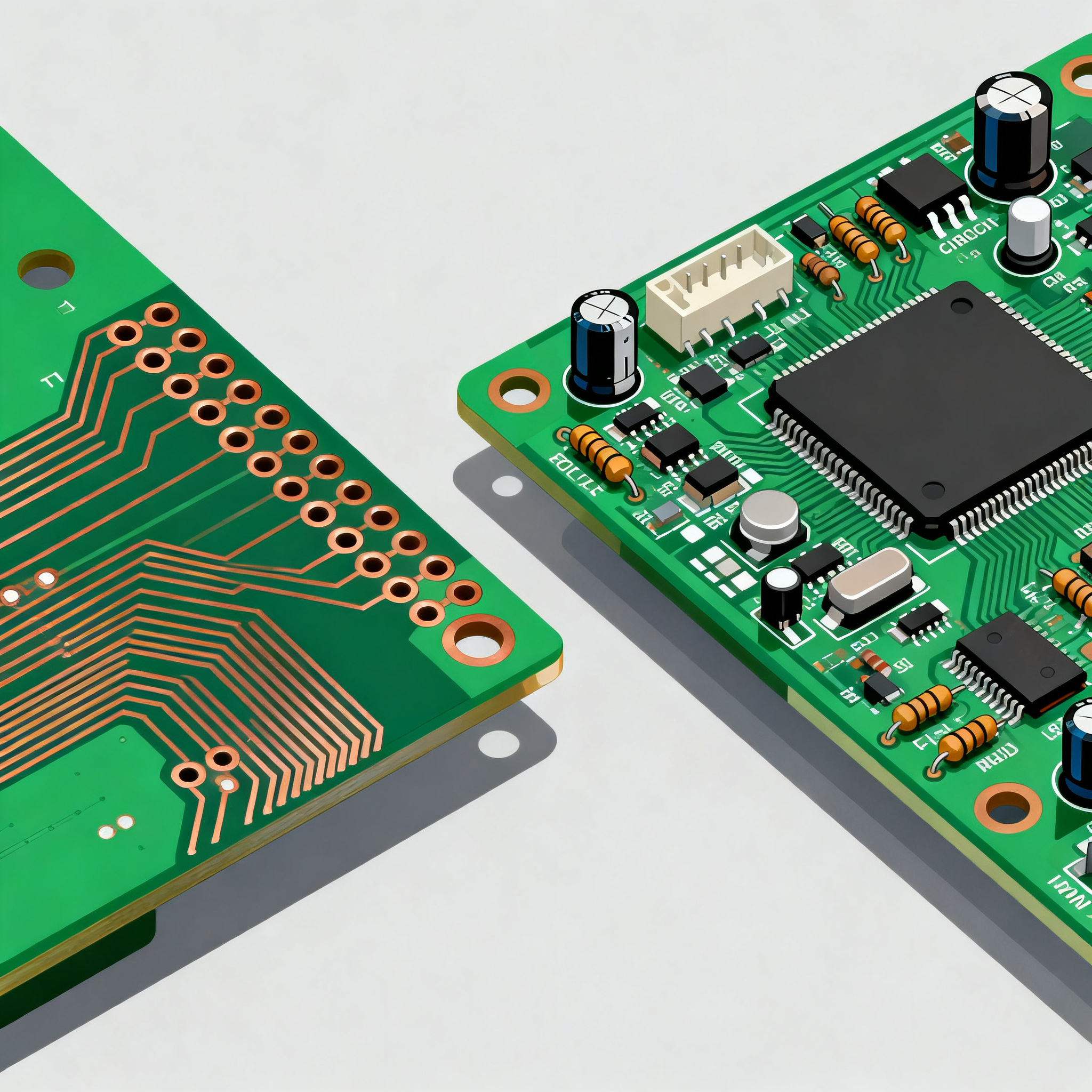
PCBs are the foundational platforms upon which electronic components are mounted. They consist of a non-conductive substrate, typically made from fiberglass, epoxy, or other composite materials, with conductive pathways etched onto them. These pathways, or traces, allow for the electrical connection of various components. On the other hand, PCBAs include the assembly of components onto the PCB, transforming it into a functional circuit board. This process involves soldering components such as resistors, capacitors, and integrated circuits onto the PCB, thus completing the electrical circuit.
The architecture and principles of PCBs and PCBAs are governed by industry standards such as IPC-A-610 and IPC-2221. These standards ensure uniformity in design, manufacturing, and quality inspection, providing a benchmark for engineers to follow. Understanding these core concepts is essential for achieving high-performance and reliable electronic assemblies.
Detailed Specifications
When evaluating PCBs and PCBAs, several specifications are paramount. These include parameters such as layer count, material type, copper thickness, and trace width, which influence the board's electrical and thermal performance. Additionally, understanding the ratings for temperature, voltage, and current is critical for ensuring that the board can handle the intended application. Engineers must carefully assess these specifications to select the appropriate components for their designs.
| Parameter | PCB Specification | PCBA Specification |
|---|---|---|
| Layer Count | 1-16 layers | 1-16 layers |
| Material Type | FR-4, CEM-3 | FR-4, CEM-3 |
| Copper Thickness | 1 oz/sq ft | 1 oz/sq ft |
| Trace Width | 3 mils minimum | 3 mils minimum |
| Temperature Rating | -40°C to 110°C | -40°C to 110°C |
| Voltage Rating | Up to 600V | Up to 600V |
| Current Rating | Up to 5A | Up to 5A |
| Surface Finish | HASL, ENIG | HASL, ENIG |
| Solder Mask Color | Green, Blue | Green, Blue |
| Minimum Drill Size | 0.1 mm | 0.1 mm |
| Impedance Control | Yes | Yes |
Key Takeaways from the Specifications
The specifications outlined above provide a comprehensive view of the critical parameters that define PCBs and PCBAs. The layer count and material type are pivotal in determining the board's complexity and application suitability. For instance, multi-layer boards are ideal for complex circuits, while the material type influences thermal and mechanical properties. Copper thickness and trace width are crucial for managing current capacity and minimizing resistance. Engineers must ensure that these specifications align with their design requirements to achieve optimal performance and reliability.
| Characteristic | PCB Performance | PCBA Performance |
|---|---|---|
| Thermal Conductivity | 0.3 W/mK | 0.3 W/mK |
| Dielectric Constant | 4.2-4.7 | 4.2-4.7 |
| Loss Tangent | 0.02 | 0.02 |
| Maximum Power | 10W | 10W |
| Signal Integrity | High | High |
| Thermal Expansion | 14-17 ppm/°C | 14-17 ppm/°C |
| Moisture Absorption | 0.1% | 0.1% |
| Thermal Shock Resistance | Excellent | Excellent |
| Electrical Conductivity | Good | Good |
| ESD Protection | Standard | Standard |
Practical Implications
The performance metrics of PCBs and PCBAs are instrumental in determining their suitability for various applications. Thermal conductivity and expansion are vital for managing heat dissipation and ensuring stability under temperature fluctuations. The dielectric constant and loss tangent affect signal integrity, which is crucial for high-frequency applications. Engineers should consider these metrics when designing circuits for specific environments, ensuring that the board can withstand operational stresses and maintain performance.
| Application | PCB Configuration | PCBA Configuration |
|---|---|---|
| Consumer Electronics | 4-layer, FR-4 | 4-layer, FR-4, SMD components |
| Automotive | 8-layer, High-Tg | 8-layer, High-Tg, THT & SMD |
| Industrial Control | 6-layer, CEM-3 | 6-layer, CEM-3, Mixed assembly |
| Telecommunications | 12-layer, Low-loss | 12-layer, Low-loss, RF components |
| Medical Devices | 10-layer, Biocompatible | 10-layer, Biocompatible, Precision assembly |
| Aerospace | 16-layer, High-density | 16-layer, High-density, Mil-spec components |
| Wearable Technology | 2-layer, Flexible | 2-layer, Flexible, Miniature components |
Application Guidelines
The application matrix provides insight into how different PCB and PCBA configurations cater to specific industry needs. For example, consumer electronics often use 4-layer boards with SMD components for compact designs, while automotive applications require high-Tg materials for thermal resilience. In telecommunications, low-loss materials are critical for RF applications. Engineers should leverage this data to align their design choices with industry-specific requirements, ensuring that their products meet performance and reliability standards.
Design Considerations
When designing PCBs and PCBAs, engineers must consider several factors to optimize performance and manufacturability. Key considerations include:
- Trace Layout: Proper trace layout is crucial for minimizing interference and ensuring signal integrity. Engineers should adhere to design rules that specify trace width, spacing, and routing paths.
- Component Placement: Strategic component placement minimizes signal path lengths and reduces parasitic effects. Critical components should be placed to optimize thermal management and accessibility for testing.
- Thermal Management: Effective heat dissipation is essential for reliability. Engineers should incorporate thermal vias, heat sinks, and copper pours to manage heat distribution.
- Impedance Control: For high-frequency applications, maintaining controlled impedance is necessary to prevent signal reflection and loss. This involves precise trace dimensions and dielectric material selection.
- Power Distribution: A robust power distribution network minimizes voltage drops and ensures stable operation. Engineers should use wide traces and multiple vias for power and ground connections.
- Design for Manufacturability (DFM): DFM principles ensure that designs are compatible with manufacturing processes. This includes considering panelization, solder mask clearance, and assembly tolerances.
Step-by-Step Implementation
- Define Requirements: Start by outlining the functional and performance requirements of the PCB/PCBA. This includes electrical, thermal, and mechanical specifications.
- Schematic Design: Create a schematic diagram that captures the electrical connections and component relationships. Use CAD software to ensure accuracy and completeness.
- PCB Layout: Translate the schematic into a PCB layout, considering trace routing, component placement, and layer stack-up. Pay attention to design rules and constraints.
- Design Verification: Conduct design rule checks (DRC) and electrical rule checks (ERC) to identify potential issues. Simulate the design to validate performance metrics.
- Prototype Fabrication: Manufacture a prototype PCB to evaluate design feasibility. Work with a reputable PCB manufacturer to ensure quality and reliability.
- Assembly and Testing: Assemble the prototype with components, followed by rigorous testing to verify functionality, performance, and compliance with specifications.
- Iterate and Optimize: Analyze test results to identify areas for improvement. Make necessary design adjustments and iterate the process to enhance performance and manufacturability.
- Final Production: Once satisfied with the prototype, proceed with final production. Implement quality control measures to ensure consistent outcomes.
Common Issues & Solutions
Even with meticulous planning, issues can arise during PCB/PCBA design and manufacturing. Here are some common problems and their solutions:
- Signal Integrity Problems: Caused by poor trace routing or impedance mismatch. Solution: Use controlled impedance techniques and proper trace layout.
- Thermal Management Issues: Overheating due to inadequate heat dissipation. Solution: Incorporate thermal vias, heat sinks, and optimize copper pours.
- Manufacturing Defects: Include solder bridges and misaligned components. Solution: Follow DFM guidelines and conduct thorough inspections.
- Component Failures: Result from incorrect component ratings or assembly errors. Solution: Verify component specifications and use automated assembly processes.
- EMI/EMC Challenges: Electromagnetic interference affecting circuit performance. Solution: Implement shielding, filtering, and proper grounding techniques.
- Power Distribution Issues: Voltage drops and instability in power supply. Solution: Design a robust power distribution network with adequate trace width and vias.
Applications & Use Cases
PCBs and PCBAs are integral to a wide range of applications across various industries:
- Consumer Electronics: Smartphones, laptops, and home appliances rely on compact and efficient PCB designs.
- Automotive: Advanced driver-assistance systems (ADAS) and infotainment systems use high-reliability PCBAs.
- Medical Devices: Diagnostic equipment and wearable health monitors require precision and biocompatible materials.
- Aerospace: Avionics and satellite systems demand high-density and mil-spec compliant PCBs.
- Industrial Automation: Control systems and robotics use robust PCBs for harsh environments.
Selection & Sourcing Guide
Choosing the right PCB/PCBA supplier is crucial for project success. Consider factors such as manufacturing capabilities, lead times, and quality certifications. For sourcing components, visit IC Online for a comprehensive selection of electronic components and suppliers.
FAQ
- What is the difference between a PCB and a PCBA? A PCB is the bare board, while a PCBA includes all the assembled components, making it a functional circuit.
- Why is layer count important in PCBs? Layer count affects the complexity and capability of the board to handle intricate circuits and high-speed signals.
- How does material type influence PCB performance? Material type determines thermal and electrical properties, affecting heat management and signal integrity.
- What is impedance control, and why is it necessary? Impedance control ensures consistent signal transmission, preventing reflections and losses in high-frequency circuits.
- How can I improve thermal management in PCB design? Use thermal vias, heat sinks, and optimize copper areas to enhance heat dissipation.
- What are common manufacturing defects in PCBAs? Defects include solder bridges, misaligned components, and poor solder joints, often mitigated by following DFM principles.
- How do I ensure ESD protection in my PCB design? Implement proper grounding, use ESD-safe components, and consider protective coatings.
- What role does IPC standards play in PCB design? IPC standards provide guidelines for design, manufacturing, and quality assurance, ensuring industry compliance.
- Can I use the same PCB design for different applications? While possible, application-specific requirements may necessitate design modifications to meet performance standards.
Conclusion
PCBs and PCBAs are fundamental to the electronics industry, and understanding their specifications, performance metrics, and applications is vital for engineers seeking precision. By adhering to industry standards, leveraging detailed specifications, and applying practical design considerations, engineers can achieve high-performance and reliable electronic assemblies. This comprehensive guide serves as a valuable resource for navigating the complexities of PCB and PCBA design, ensuring successful project outcomes.