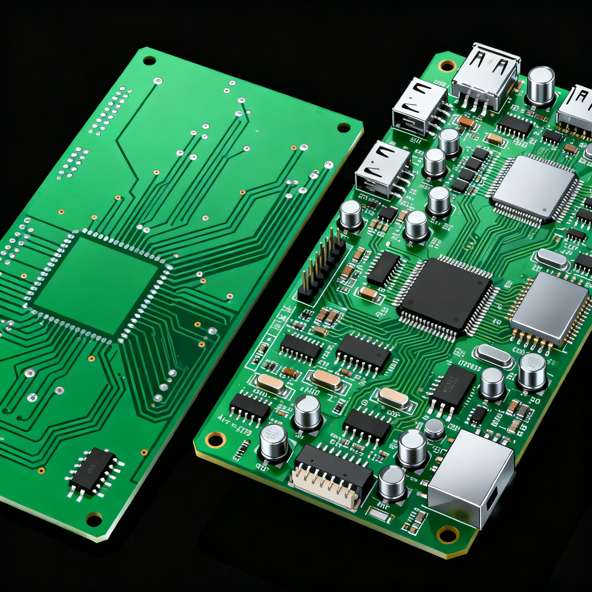
PCB vs PCBA: 5 Troubleshooting Pitfalls When Ordering 4-Layer Bare Boards vs Assembled Units
When Bare Board Contamination and Material Shortages Collide: Why the PCB vs PCBA Decision Matters Now Engineers and buyers who treat the PCB-vs-PCBA choice as a simple logistics split are walking int...
When Bare Board Contamination and Material Shortages Collide: Why the PCB vs PCBA Decision Matters Now
Engineers and buyers who treat the PCB-vs-PCBA choice as a simple logistics split are walking into two accelerating problems. The first is ionic contamination — residues from salts, oils, dust, and process chemistry that sit on a bare board long before the first component is placed. As MCL stresses, these contaminants often originate from a lack of bare board cleanliness, and they don’t always announce themselves until a finished assembly fails humidity cycling, exhibits leakage currents, or develops intermittent shorts under conformal coating. The second pressure is laminate supply volatility. DeDesignWorks notes that R-4 and copper-clad laminate shortages have made lead times lumpy, especially for custom 4‑layer stackups — and the only way to avoid a schedule crash is to design supply‑chain risk management in from day one, not at the backend when production builds are already queued.
The intersection of these trends means the decision to order a bare 4‑layer board or a turnkey assembled unit is no longer just about price. It is a frontline troubleshooting lever. Even microscopic defects at the board level — solder cracks, misplaced passives, contamination trapped under components — can cascade into field failures that damage a brand’s reputation and trigger expensive recalls, as JLCPCB points out. When you control the boundary between fabrication and assembly, you control the fault chain. When you don’t, you inherit every gap in cleanliness, handling, and inspection that exists between two suppliers who may never speak to each other. That is why leaning into the PCB vs PCBA question before quoting is not over‑engineering — it is the cheapest insurance you can buy.
The Hidden Price Tag of a 4‑Layer Stackup: What Bare Board Specs Mean for Assembly Success
On paper, a 4‑layer PCB is the cost‑performance sweet spot for designs that need continuous reference planes, cleaner power distribution, and tighter impedance control than a 2‑layer board can offer. Suga PCBA describes it as the logical step when a 2‑layer layout cannot accommodate the necessary routing and plane integrity, and Leadsintec confirms it remains the most widely used multilayer structure in consumer and industrial electronics. But the moment you shift from an assembled unit order to a bare‑board‑only purchase, the cost model changes in ways that assembly success depends on.
The processing cost of a 4‑layer board is inherently higher because the inner layers are laminated together under heat and pressure, as NextPCB explains. That premium is only the start. When you order bare boards, every specification you choose — copper weight, high‑Tg FR‑4 versus standard Tg, impedance coupons, tight registration, and surface finish area — rides on a more expensive traveler. Aivon underscores that 2‑oz inner copper or extra surface finish acreage adds cost more steeply on a 4‑layer stack than on a simpler 2‑layer board. Meanwhile, bare boards arrive with the cleanliness level that the fabricator chose, not necessarily what your assembly process needs. That directly influences ionic contamination risk, per MCL, because residues from the board itself become the root cause of latent failures after soldering.
The table below quantifies what changes when you compare a bare 4‑layer order with a turnkey PCBA order, highlighting the contamination and schedule vectors that often get ignored until test fails.
| Parameter | Bare 4‑Layer PCB | Turnkey PCBA (Fab + Assembly) | Impact on Contamination & Schedule Risk |
|---|---|---|---|
| Lead time (standard) | 3–5 business days typical for quick‑turn 2–4 layers (SBC) | 5–15 business days, heavily dependent on component availability | Bare board speed is meaningless if missing components idle boards in uncontrolled storage, inviting moisture and contamination uptake. |
| Cost drivers | Laminate, copper weight, surface finish, impedance control, tight registration (Aivon) | BOM cost, assembly labor, NRE, test coverage | Over‑specifying a bare board without assembly validation can inflate cost without improving reliability; an assembled unit lets you align tolerances end‑to‑end. |
| Cleanliness ownership | Fabricator’s final wash process; often no ionic cleanliness data provided | Assembly partner controls incoming board condition and can perform pre‑assembly cleaning and ROSE testing | Bare boards shipped without cleanliness certification shift the contamination risk entirely onto assembly — a gap that causes field failures (MCL). |
| Handling environment | Packaging and shipping; ESD control is fabricator‑dependent | Controlled ESD‑safe environment throughout manufacturing (Matric) | Boards that absorb moisture or suffer ESD strikes before assembly create latent defects that pass initial test but fail in the field. |
| Laminate supply risk | Subject to R‑4 and prepreg allocations (DeDesignWorks) | Shared risk; turnkey partner carries the inventory buffer and re‑qualification burden | A bare board order that gets stalled waiting for a specific prepreg can freeze the entire project, while a turnkey house can often re‑source within qualified constraints. |
Stackup choices multiply these dynamics. Moving from a standard FR‑4 4‑layer with 0.5‑oz inner copper to a high‑Tg variant with 2‑oz planes and controlled‑impedance traces — a configuration detailed by FS Circuits — stretches both lead times and fabrication tolerances. When all the technical risk sits with a bare board supplier who only sees a Gerber file, the assembly step inherits every un‑validated assumption about laminate behavior during reflow, solder mask adhesion, and hole wall quality. That is what makes the turnkey route, where a single entity engineers the entire chain from laminate to final test, a de‑risking move even when it looks slightly more expensive on a bill of materials line item.
Bare Board or Turnkey Assembly: A Side‑by‑Side Look at Lead Times, Cost Drivers, and Hidden Risks
The decision tree splits on more than unit price. Real‑world projects break on lead‑time predictability, contamination containment, and who carries the liability when something invisible goes wrong. Below is a direct comparison of a bare 4‑layer PCB order shipped to an in‑house assembly line versus a turnkey PCBA sourced from a single contract manufacturer.
| Comparison Metric | Option A: Bare 4‑Layer PCB + In‑House Assembly | Option B: Turnkey PCBA (Single Supplier) | Selection Criteria & Failure Boundary |
|---|---|---|---|
| Lead‑time certainty | 3–5 days for bare boards (SBC); total schedule depends on in‑house capacity and component stocks | 5–15 business days quoted upfront, with component lead times baked in | Option A wins only if your factory is never bottlenecked and your BOM is 100% on hand. One delayed reel turns bare boards into contamination‑prone inventory. |
| Cost at low volume (1–500 units) | Lower bare board cost, but hidden charges for handling, cleaning, and yield loss not always accounted | Higher NRE and assembly cost but predictable, with yield and test owned by the supplier | At low volume, the cost of one re‑spin due to ionic contamination or ESD damage can erase any savings from splitting the order. |
| Ionic contamination risk | Falls on the gap between fabricator and in‑house cleaning; rarely measured before reflow | Supplier can enforce incoming ROSE testing and pre‑assembly wash as standard if written into the contract | MCL confirms residues left on bare boards become the primary source of post‑assembly leakage; Option B closes that gap. |
| ESD and handling integrity | Dependent on in‑house protocols, storage conditions, and operator discipline | Select a CM that uses ESD‑safe protocols as standard — anti‑static tools, controlled environments — to prevent latent damage (Matric) | Option B with a qualified partner reduces variability; one dry‑air day in an uncontrolled stockroom can degrade Option A’s entire batch. |
| Supply‑chain risk and re‑work flexibility | Split sourcing; BOM risk must be designed in from day one with continuous risk review (DeDesignWorks) | Turnkey supplier manages allocations and may re‑qualify alternates faster | Option A works for mature designs with stable, multi‑sourced BOMs. First‑run or custom‑laminate builds lean heavily toward Option B to avoid schedule black holes. |
| Rework feasibility | Inner‑layer defects cannot be reworked; the board is scrap | Single supplier catches inner‑layer opens/shorts at bare‑board test and can adjust the panel before assembly | Any undetected inner‑layer flaw in Option A becomes a field‑failure lottery because post‑assembly rework is impossible on 4‑layer buried vias. |
The fork in the road often comes down to who carries the risk of the in‑between state — that period from when bare boards leave the fabricator until they are populated. In a split‑sourcing model, that risk is yours. You must validate ionic cleanliness on incoming lots, manage ESD‑safe unpacking and storage, and absorb the cost of boards that fail post‑reflow due to contamination that arrived with the laminate. Turnkey models push that responsibility onto the partner, and the best ones treat cleanliness not as a customer‑requested add‑on but as a standard process step. For many teams, especially those without a dedicated failure analysis lab, that shift in ownership is worth the premium.
5 Troubleshooting Pitfalls When Ordering 4‑Layer Bare Boards vs Assembled Units
The following table captures the five most common failure modes that separate a smooth launch from an expensive recall, along with actionable checks that engineering and procurement can use at the quoting stage.
| Pitfall # | Pitfall Description | Trigger Checklist (Actionable) | Mitigation |
|---|---|---|---|
| 1 | Ionic contamination from residual board salts and oils — traces left during fabrication that turn into leakage paths after soldering (MCL) |
|
Require ROSE test reports ≤1.56 µg/cm² NaCl equivalence and add a factory audit of the fabricator’s final wash process. When ordering turnkey, write cleanliness milestones into the acceptance criteria. |
| 2 | ESD or handling damage during bare board storage and assembly — latent ESD strikes that degrade semiconductor interfaces (Matric) |
|
Choose a contract manufacturer that lists ESD‑safe protocols as a standard capability, not an option. If assembling in‑house, implement daily ESD audits and quarantine any batch that exceeds the allowable exposure window. |
| 3 | Laminate shortages that extend lead times unpredictably — especially for custom 4‑layer stacks that depend on specific prepreg types (DeDesignWorks) |
|
Design supply‑chain resilience in from the schematic: pre‑qualify two laminate vendors, maintain a live BOM risk review, and use turnkey partners that hold consignment stock for regular runs. |
| 4 | Cost overruns from overlooked copper weight, registration, or surface‑finish specs — small changes that balloon on a 4‑layer traveler (Aivon) |
|
Freeze specifications at the minimum that guarantees assembly yield. Every “nice‑to‑have” parameter adds cost on a 4‑layer traveler; negotiate with the turnkey partner to see if post‑laminate trimming can relax a tight callout without hurting function. |
| 5 | Solder cracks, wrong passives, or misalignment that escape visual inspection until post‑assembly test — microscopic defects that accumulate into field failures (JLCPCB) |
|
Demand in‑process inspection data, not just a pass/fail sticker. For turnkey orders, specify that test coverage must include at least flying‑probe or ICT on 100% of units, with root‑cause analysis for any repeat defect. |
Each pitfall traces back to a moment where information or ownership was handed off. When you order bare 4‑layer boards and manage assembly elsewhere, the checklist items above become your responsibility, often across two or three different companies that communicate through purchase orders. Turnkey assembly does not magically erase these failure modes, but it does consolidate accountability. The CM that fabricates the bare board and populates it in‑house has a direct incentive to get contamination, handling, and component placement right, because they own the test fallout. That single‑throat‑to‑choke reality is why many engineering teams are moving away from split‑source for anything beyond mature, high‑volume platforms where every variable has been wrung out over thousands of cycles.
Questions Engineers Ask Before Committing to a 4‑Layer Bare or Assembled Order
Q: When does it make sense to order bare 4‑layer PCBs instead of complete assemblies?
It makes sense when you have a trusted in‑house assembly line with proven, audited cleanliness protocols and the board is a standard, high‑volume design with stable component availability. If any of those conditions isn’t rock‑solid, the risk of ionic contamination, ESD damage, or mismatched tolerance stacks usually outweighs the per‑unit cost saving. Factor in the engineering hours spent chasing root causes across fabricator and assembly house — the “cheaper” bare‑board order can become the most expensive decision in the project.
Q: How can I check if an assembly partner will handle my bare 4‑layer boards correctly?
Ask for documented ESD‑safe procedures and ionic cleanliness test data — specifically ROSE testing or SIR reports on their incoming boards. Review their incoming inspection criteria for laminate condition, copper weight, and registration against your IPC‑6012 class. A manufacturer that lists cleanliness as a standard protocol, not a special request, is a safer bet. Matric offers a concise mitigation tip: choose a contract manufacturer that uses ESD‑safe protocols, anti‑static tools, and controlled environments as standard, with stringent cleanliness protocols throughout assembly. That is the baseline, not the upgrade.
Q: What are early warning signs of ionic contamination in assembled 4‑layer boards?
In‑circuit test anomalies under humidity, slight but steady leakage currents, or intermittent shorts that appear only after conformal coating are classic red flags. Visually, white residues near vias or under BGA keep‑out areas often indicate leftover flux or plating salts. MCL notes that the root cause frequently traces back to board‑level residues present before the first component was placed, which is why treating the bare board as clean by default is a dangerous assumption.
Q: How do material shortages specifically hit 4‑layer PCBs compared to simpler boards?
4‑layer boards rely on consistent supplies of R‑4 laminate and specific prepreg/thick copper sheets. Substitute materials often require requalification that eats weeks, and vendor allocations tend to favor high‑volume commodity stacks, leaving custom stackups with longer, lumpier lead times. DeDesignWorks advises that supply‑chain risk has to be designed in from day one — this means pre‑qualifying laminate alternatives and keeping communication open with pre‑qualified vendors. Without that, a 4‑layer build can stall for a single missing prepreg while 2‑layer boards sail through.
Q: Should I split the PCB order and assembly supplier to cut costs on a 4‑layer build?
It can work for straightforward, mature designs with tightly managed BOMs where you have full visibility into component inventories and a proven incoming cleaning process. For a first‑run or low‑volume project, a single turnkey partner who owns the full process reduces the risk of finger‑pointing when a failure occurs. JLCPCB points out that even small placement or soldering defects can cascade into field failures, and when two suppliers are involved, determining whether the fault originated in laminate, soldering, or passive placement becomes a slow, expensive forensic exercise.
Q: What lead time should I expect for 4‑layer bare boards alone, and how do I buffer for PCBA component delays?
Standard 4‑layer bare boards can arrive in 3–5 business days from a quick‑turn shop, according to SBC. Once assembly planning begins, component lead times dominate the schedule. Always add a 2–3 week buffer and maintain a live BOM risk review, especially for 4‑layer boards where inner‑layer rework is impossible. A late‑arriving BGA, crystal, or power regulator doesn’t just delay assembly — it turns finished bare boards into shelf stock that can accumulate moisture and contamination, effectively resetting the reliability clock.
References & Further Reading
- MCL PCB Issue Guide: PCB Failure Analysis and Common Issues
- Matric Group: 6 Common Causes of PCB Failure
- DeDesignWorks: PCB Material Shortages in 2026
- JLCPCB: PCB Failure Analysis — Understanding the Causes and Solutions
- SBC Inc: What Are the Differences Between PCB and PCBA?
- Aivon: 2‑Layer vs 4‑Layer FR4 PCB Cost, Performance, and Design Differences
- NextPCB: 2‑Layer or 4‑Layer PCB? Don’t Let a Few Dollars Difference Ruin Your Circuit Prototype
- Suga PCBA: 4 Layer PCB Guide — Layers, Stackups and Design Choices
- Leadsintec: Complete Guide to 4‑Layer PCBs
- FS Circuits: 4 Layer PCB Stackup — Design Rules and Manufacturing
The five pitfalls outlined above share a common thread: they all exploit the gap between a bare board’s intended design and the real‑world conditions it encounters before power‑up. Whether your path leads to split sourcing or a turnkey assembly partner like NovaPCBA, closing that gap is what separates a board that merely passes test from one that survives years in the field. If you are weighing a 4‑layer PCB vs PCBA order and want the reliability math done before you hit purchase, our team can walk you through the stackup, cleanliness, and BOM decisions that match your production reality.