pcb production lead times
PCB Production Lead Times and Design Considerations table { border-collapse: collapse; width: 100%; margin: 20px 0; } th, td { border: 1px solid #ddd; padding: 8px; } th { background: #f0f0f0; } Intro...
Introduction
In the rapidly evolving world of electronics, printed circuit boards (PCBs) serve as the backbone of electronic devices, from simple consumer gadgets to complex industrial systems. Understanding PCB production lead times is crucial for designers and manufacturers aiming to optimize their production cycles and reduce time-to-market. This article delves into the intricacies of PCB design rules, stackup design, signal integrity, and manufacturing considerations, providing a comprehensive overview for both novice and seasoned engineers.
Technical Overview
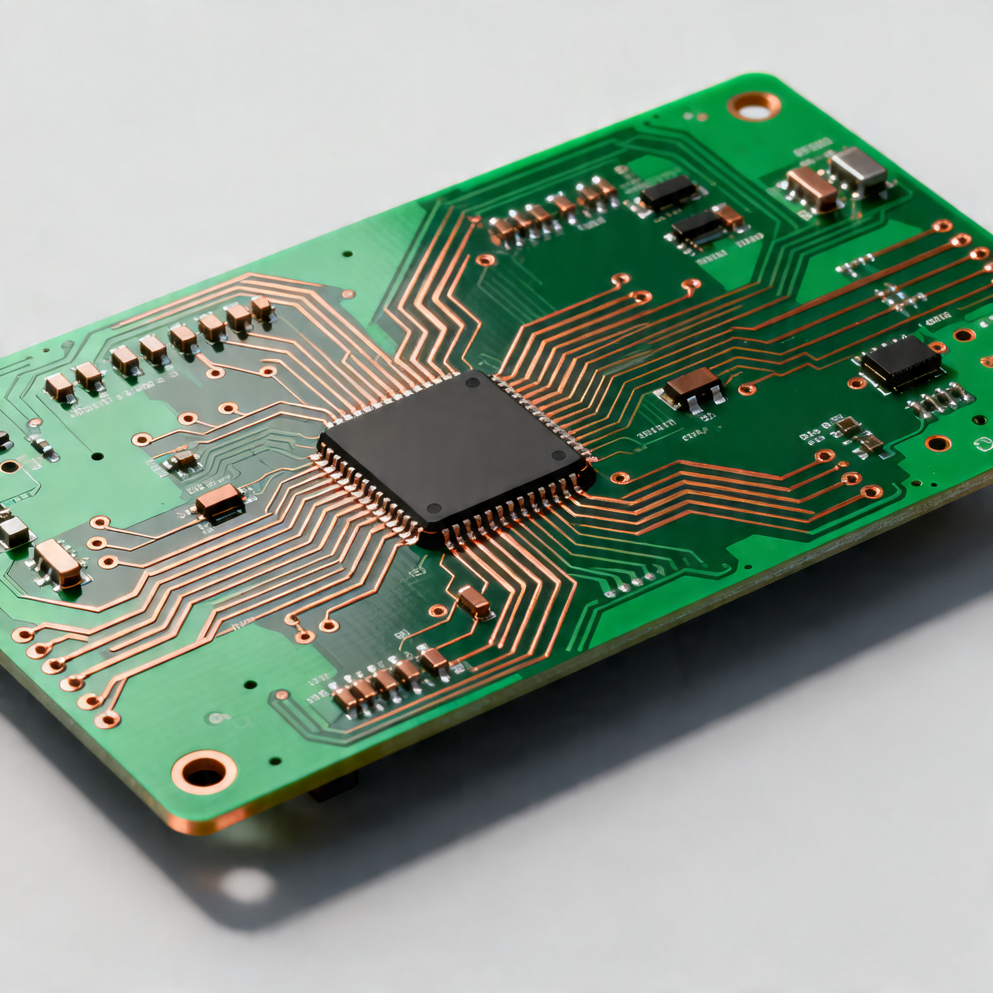
PCBs are intricate components that require meticulous design and manufacturing processes. The architecture of a PCB involves multiple layers that serve different purposes, such as signal routing, power distribution, and grounding. Key principles include the management of signal integrity to prevent data loss and interference, as well as the consideration of thermal management to ensure the longevity and reliability of the board. Understanding these core concepts is essential for creating efficient and effective PCB designs that meet industry standards and performance requirements.
Detailed Specifications
Specifications are the foundation of any PCB design, dictating the rules and guidelines that ensure the board functions as intended. These specifications include trace widths, spacing, via sizes, and clearances, which are critical for maintaining signal integrity and ensuring manufacturability. Proper adherence to these specifications is vital for achieving a balance between performance and cost-effectiveness.
| Design Rule | Minimum Value | Recommended Value |
|---|---|---|
| Trace Width | 4 mils | 6 mils |
| Trace Spacing | 4 mils | 8 mils |
| Via Hole Size | 0.2 mm | 0.3 mm |
| Via Pad Diameter | 0.4 mm | 0.6 mm |
| Clearance to Edge | 0.5 mm | 1.0 mm |
| Annular Ring | 0.1 mm | 0.15 mm |
| Drill to Copper | 0.2 mm | 0.25 mm |
| Solder Mask Clearance | 0.1 mm | 0.15 mm |
| Silkscreen Line Width | 0.1 mm | 0.15 mm |
| Component Pad Size | 0.5 mm | 0.7 mm |
Key Takeaways from the Specifications
The design rules outlined above are crucial for ensuring PCB manufacturability and performance. For instance, trace width and spacing play a significant role in determining the current-carrying capacity and signal integrity of the board. Adhering to the recommended values helps minimize the risk of manufacturing defects and signal interference. Additionally, proper via sizing and pad diameters ensure reliable connections between layers, which is vital for multi-layer PCBs. These specifications provide a framework for balancing cost, performance, and manufacturability in PCB design.
| Layer Configuration | Signal Layers | Ground/Power Layers |
|---|---|---|
| 2-Layer | 2 | 0 |
| 4-Layer | 2 | 2 |
| 6-Layer | 4 | 2 |
| 8-Layer | 6 | 2 |
| 10-Layer | 8 | 2 |
| 12-Layer | 10 | 2 |
| 14-Layer | 12 | 2 |
| 16-Layer | 14 | 2 |
Practical Implications
The choice of layer stackup configuration significantly impacts the performance and cost of a PCB. Higher layer counts allow for more complex routing and better signal integrity due to dedicated ground and power planes. However, they also increase manufacturing complexity and cost. Designers must weigh these factors against the requirements of their specific application, balancing the need for performance with budget constraints. Understanding the implications of different layer configurations helps in making informed decisions that align with project goals.
| Material | Dielectric Constant (Dk) | Loss Tangent (Df) |
|---|---|---|
| FR-4 | 4.5 | 0.020 |
| Rogers 4350B | 3.66 | 0.0037 |
| Rogers 4003C | 3.38 | 0.0027 |
| Isola FR408HR | 3.67 | 0.009 |
| Nelco N4000-13 | 3.7 | 0.015 |
| Arlon 85N | 3.5 | 0.0025 |
| Megtron 6 | 3.4 | 0.002 |
| Isola PCL370HR | 3.7 | 0.005 |
| Shengyi S1000-2 | 4.2 | 0.018 |
Application Guidelines
The choice of PCB material is critical for achieving the desired electrical performance and reliability. Materials like FR-4 are widely used due to their cost-effectiveness and versatility, but they may not be suitable for high-frequency applications where materials like Rogers or Megtron offer superior performance. The dielectric constant and loss tangent values influence signal speed and loss, making them key factors in material selection. Engineers must consider these properties in relation to their application's frequency requirements and environmental conditions.
Design Considerations
Effective PCB design involves a careful balance of several factors, including electrical, thermal, and mechanical considerations. Signal integrity is paramount, requiring attention to trace impedance, length matching, and termination methods. Thermal management is another critical aspect, as heat dissipation can affect component performance and longevity. Designers must also consider mechanical constraints such as board size, shape, and mounting methods. By addressing these considerations, engineers can create PCBs that meet performance specifications while remaining manufacturable and cost-effective.
Step-by-Step Implementation
- Define Requirements: Begin by outlining the functional and performance requirements of the PCB, including electrical, thermal, and mechanical constraints.
- Schematic Design: Create a detailed schematic that captures all electrical connections and components, ensuring accuracy and completeness.
- Component Selection: Choose components that meet the design requirements, considering factors such as availability, cost, and performance.
- PCB Layout: Design the PCB layout, adhering to design rules for trace width, spacing, and via sizes, while optimizing for signal integrity and thermal management.
- Layer Stackup Design: Select an appropriate layer stackup configuration that balances performance and cost, considering signal routing and power distribution needs.
- Material Selection: Choose PCB materials based on dielectric properties and loss characteristics, aligning with the application's frequency and environmental requirements.
- Simulation and Verification: Use simulation tools to verify signal integrity, thermal performance, and mechanical robustness, making necessary adjustments.
- Prototype and Testing: Manufacture a prototype PCB and conduct thorough testing to validate design performance and identify any issues.
Common Issues & Solutions
- Signal Integrity Problems: Ensure proper trace impedance matching and use of differential pairs to minimize reflections and crosstalk.
- Thermal Management Challenges: Incorporate thermal vias and heat sinks to effectively dissipate heat from high-power components.
- Manufacturing Defects: Adhere to design for manufacturability (DFM) guidelines to reduce the risk of defects during production.
- Component Sourcing Delays: Work with reliable suppliers and consider alternative components to mitigate supply chain disruptions.
- Mechanical Fit Issues: Perform mechanical simulations and prototyping to ensure the PCB fits within the intended enclosure and mounting system.
Applications & Use Cases
PCBs are used in a wide range of applications, from consumer electronics like smartphones and laptops to industrial equipment and automotive systems. In telecommunications, high-frequency PCBs are essential for signal processing and data transmission. In the medical field, PCBs are used in diagnostic and therapeutic devices, requiring high reliability and precision. Each application presents unique challenges and requirements, emphasizing the importance of tailored PCB design and manufacturing approaches.
Selection & Sourcing Guide
When selecting and sourcing PCBs, engineers should consider factors such as material properties, layer count, and manufacturing capabilities. Collaborating with reputable suppliers like IC Online can ensure access to high-quality components and materials, reducing the risk of delays and defects. Evaluating supplier capabilities and lead times is crucial for aligning production schedules with project timelines.
FAQ
- What is the typical lead time for PCB manufacturing? Lead times can vary from a few days to several weeks, depending on complexity and quantity.
- How do I choose the right PCB material? Consider the application's frequency, environmental conditions, and budget when selecting materials.
- What are the benefits of a multi-layer PCB? Multi-layer PCBs offer improved signal integrity and reduced electromagnetic interference.
- How can I ensure signal integrity in my PCB design? Use controlled impedance traces, differential pairs, and proper termination techniques.
- What is DFM, and why is it important? Design for manufacturability (DFM) ensures that the PCB can be manufactured efficiently and reliably.
- How do I manage heat dissipation in a PCB? Use thermal vias, copper pours, and heat sinks to effectively manage heat.
- Why is layer stackup important in PCB design? Proper stackup design optimizes signal routing and power distribution, enhancing performance.
- What are the common causes of PCB defects? Defects can arise from poor design, material selection, or manufacturing processes.
- How can I reduce PCB production costs? Optimize design for efficiency, choose cost-effective materials, and work with reliable suppliers.
- What are via-in-pad and microvias? These are advanced techniques for routing and connecting layers in high-density PCBs.
Conclusion
Understanding PCB production lead times and design considerations is vital for creating high-performance, reliable electronic devices. By adhering to design rules, selecting appropriate materials, and optimizing layer stackups, engineers can achieve efficient and cost-effective PCB designs. Collaboration with trusted suppliers and adherence to industry standards further enhances the manufacturability and quality of PCBs, ensuring successful project outcomes.