pcb manufacturing process flow
PCB Manufacturing Process Flow Introduction The world of electronics is ever-evolving, and at the heart of this technological revolution is the printed circuit board (PCB). PCBs are essential componen...
Introduction
The world of electronics is ever-evolving, and at the heart of this technological revolution is the printed circuit board (PCB). PCBs are essential components that enable the functioning of electronic devices by providing mechanical support and connecting electronic components. Understanding the intricacies of PCB design, layout, and manufacturing is crucial for engineers to produce reliable and efficient devices. This article delves into the PCB manufacturing process, focusing on layout rules, stackup design, signal integrity, and important manufacturing considerations.
Technical Overview
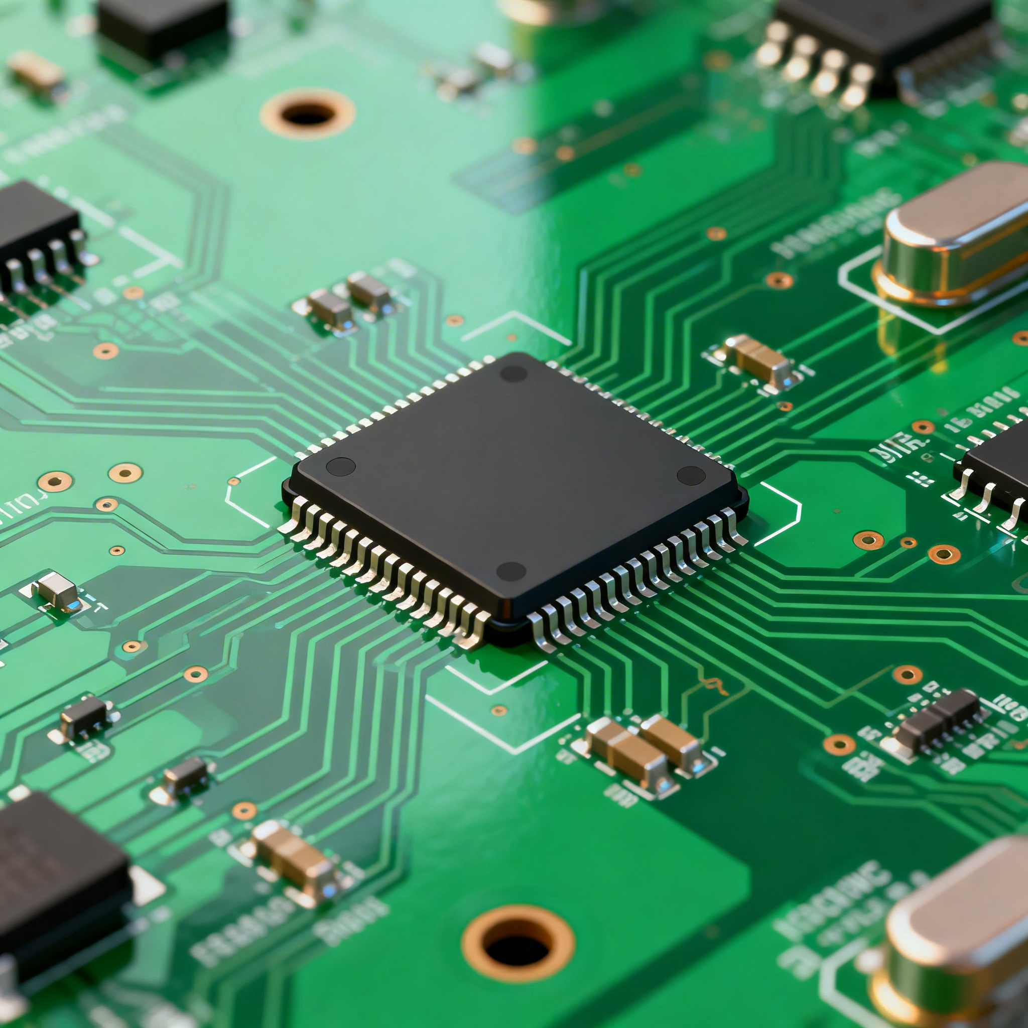
PCBs serve as the backbone for virtually all electronic devices, from simple consumer gadgets to complex industrial machinery. The process of designing and manufacturing a PCB involves several critical steps, including selecting the right materials, designing the layout, and ensuring signal integrity. The architecture of a PCB is defined by its layer stackup, which determines the board's electrical performance and mechanical properties. Key principles such as trace width, spacing, and via sizes play a significant role in ensuring that the PCB can handle the required electrical loads without interference or failure.
Detailed Specifications
When designing a PCB, several specifications must be considered to ensure optimal performance. These include trace width, spacing, via sizes, and clearances, all of which affect the board's electrical and thermal performance. Below is a comprehensive table of PCB design rules to guide engineers in creating efficient and reliable PCBs.
| Design Rule | Specification | Notes |
|---|---|---|
| Trace Width | 0.15 mm | Minimum width for signal traces |
| Trace Spacing | 0.20 mm | Minimum spacing between traces |
| Via Diameter | 0.30 mm | Standard via size for signal layers |
| Pad Size | 0.50 mm | Recommended pad size for component leads |
| Clearance | 0.25 mm | Minimum clearance from board edge |
| Annular Ring | 0.10 mm | Minimum annular ring width |
| Drill Hole Size | 0.20 mm | Minimum mechanical drill hole size |
| Solder Mask Clearance | 0.10 mm | Clearance for solder mask openings |
| Silkscreen Line Width | 0.08 mm | Minimum width for silkscreen lines |
| Component Spacing | 0.50 mm | Minimum spacing between components |
Key Takeaways from the Specifications
The specifications in the table above highlight the critical design rules that engineers must adhere to when designing a PCB. The trace width and spacing are fundamental to ensuring signal integrity, as they prevent crosstalk and signal degradation. Via sizes and pad dimensions are crucial for mechanical stability and electrical connectivity. Clearances, such as those for solder mask and board edges, ensure that the PCB can be manufactured reliably without shorts or defects. Understanding these specifications is key to designing PCBs that perform well under various operating conditions.
| Layer Configuration | Description | Applications |
|---|---|---|
| 2-Layer | Basic two-layer board | Simple circuits, low-cost applications |
| 4-Layer | Includes power and ground planes | Improved signal integrity, moderate complexity |
| 6-Layer | Signal layers with dedicated power/ground | High-performance, reduced EMI |
| 8-Layer | Advanced routing options | Complex circuits, high-speed applications |
| 10-Layer | High-density interconnects | Telecom, data centers |
| 12-Layer | Maximum routing flexibility | Advanced computing, RF applications |
Practical Implications
The choice of layer stackup is pivotal in determining the electrical performance and cost of a PCB. A 2-layer configuration is suitable for simple, cost-sensitive applications, whereas a 4-layer stackup is often used to enhance signal integrity by incorporating power and ground planes. As the complexity of the circuit increases, more layers are required to manage routing challenges and electromagnetic interference (EMI). High-layer count boards, such as 10 or 12 layers, offer the utmost flexibility and are essential for high-speed and high-frequency applications, where signal integrity is paramount.
| Material Type | Dielectric Constant (εr) | Loss Tangent (tan δ) |
|---|---|---|
| FR-4 | 4.5 | 0.020 |
| Rogers 4350B | 3.66 | 0.0037 |
| Rogers 4003C | 3.55 | 0.0027 |
| Isola 370HR | 4.04 | 0.019 |
| Nelco N4000-13 | 3.90 | 0.016 |
| Taconic TLY | 2.20 | 0.0009 |
| Polyimide | 3.5 | 0.004 |
| Arlon 85N | 3.5 | 0.0035 |
| PTFE | 2.1 | 0.0005 |
Application Guidelines
The selection of PCB materials is a critical factor that influences the board's performance and reliability. FR-4 is a commonly used material due to its balance of cost and performance. However, for high-frequency applications, materials like Rogers 4350B and PTFE offer lower dielectric constants and loss tangents, minimizing signal loss and distortion. Engineers should consider the dielectric constant and loss tangent when selecting materials, as these properties affect signal speed and attenuation. The choice of material should align with the specific requirements of the application, whether it be for consumer electronics, telecommunications, or aerospace.
Design Considerations
Designing a PCB requires careful consideration of various factors to ensure functionality and manufacturability. Signal integrity is a major concern, particularly in high-speed circuits, where proper trace impedance and controlled dielectric properties are vital. Component placement and routing must be planned to minimize electromagnetic interference (EMI) and ensure thermal management. The selection of materials and stackup configuration should align with the intended application, balancing performance, cost, and manufacturability. Adhering to IPC standards, such as IPC-2221, ensures that design practices meet industry requirements for reliability and quality.
Step-by-Step Implementation
Creating a PCB involves several detailed steps, each critical to the final product's success. Here is a step-by-step guide to the PCB manufacturing process:
- Define Requirements: Begin by outlining the electrical and mechanical requirements of the PCB, including component specifications, operating conditions, and performance criteria.
- Schematic Design: Develop a schematic diagram that captures the electrical connections and components required for the circuit.
- PCB Layout: Use PCB design software to translate the schematic into a physical layout, optimizing component placement and routing for signal integrity and manufacturability.
- Material Selection: Choose appropriate materials based on dielectric properties, thermal performance, and cost considerations.
- Stackup Design: Configure the layer stackup to support the routing and electrical performance requirements, considering signal integrity and EMI control.
- Design Rule Check (DRC): Conduct a DRC to ensure that the layout adheres to predefined design rules and constraints.
- Prototype Fabrication: Send the design files to a PCB manufacturer for prototype fabrication, selecting a vendor with capabilities that match the design specifications.
- Testing and Validation: Test the fabricated PCB to verify electrical performance and functionality, identifying and addressing any issues before full production.
Common Issues & Solutions
During PCB design and manufacturing, several common issues can arise, each requiring specific solutions:
- Signal Integrity Problems: Mitigate by optimizing trace impedance and using appropriate materials with low loss tangents.
- Thermal Management: Address with adequate heat dissipation techniques, such as thermal vias and heat sinks.
- Electromagnetic Interference (EMI): Reduce by using ground planes and proper shielding techniques.
- Manufacturing Defects: Minimize by adhering to design rules and conducting thorough DRCs.
- Component Misalignment: Ensure accurate placement with precise assembly processes and alignment tools.
Applications & Use Cases
PCBs are integral to a wide range of applications, from consumer electronics like smartphones and laptops to industrial equipment and medical devices. In telecommunications, high-layer count PCBs are used to manage complex routing and signal integrity in networking equipment. In the automotive industry, PCBs are used in engine control units and infotainment systems, requiring robust design to withstand harsh environments. The versatility of PCBs makes them indispensable in modern technology.
Selection & Sourcing Guide
When selecting and sourcing PCBs, engineers should consider factors such as material properties, manufacturing capabilities, and vendor reliability. For comprehensive resources and component sourcing, visit IC Online for a wide selection of electronic components and PCB materials.
FAQ
- What is the importance of trace width in PCB design? Trace width affects current-carrying capacity and signal integrity, crucial for reliable performance.
- How does layer stackup influence PCB performance? Stackup configuration impacts signal integrity, EMI control, and board cost.
- Why is material selection critical in high-frequency PCBs? Materials with low dielectric constants and loss tangents minimize signal distortion at high frequencies.
- What are common causes of signal integrity issues? Poor trace impedance control and inappropriate material selection are common causes.
- How can thermal management be improved in PCB design? Implementing thermal vias and using heat sinks can enhance heat dissipation.
- What role do IPC standards play in PCB design? IPC standards ensure that design practices meet industry reliability and quality requirements.
- How can EMI be minimized in a PCB? Use ground planes, proper shielding, and optimized routing to reduce EMI.
- What is the significance of design rule checks (DRC)? DRCs ensure compliance with design rules, preventing manufacturing defects.
- How can PCB prototypes be tested effectively? Use electrical testing and functional validation to identify and rectify issues.
- What factors should be considered when selecting a PCB manufacturer? Consider capabilities, quality standards, and turnaround times when choosing a manufacturer.
Conclusion
Understanding the PCB manufacturing process is crucial for engineers to design and produce reliable electronic devices. By adhering to design rules, selecting appropriate materials, and considering stackup configurations, engineers can optimize signal integrity and manufacturability. With a focus on practical design guidelines and a step-by-step implementation approach, this article provides a comprehensive overview of PCB manufacturing, equipping engineers with the knowledge to tackle complex design challenges effectively.