PCB Layout Design Rules: Critical Considerations for 6-Layer Multi-Functional Boards
PCB Layout Design Rules: Critical Considerations for 6-Layer Multi-Functional Boards Introduction In the rapidly advancing field of electronics, the design of multi-functional printed circuit boards (...
Introduction
In the rapidly advancing field of electronics, the design of multi-functional printed circuit boards (PCBs) is becoming increasingly complex. The demand for compact, high-performance devices necessitates careful consideration of PCB layout design rules, especially for 6-layer boards that support a wide range of functionalities. These boards are integral to modern electronics, providing the backbone for everything from consumer gadgets to industrial machinery. Understanding the critical considerations in PCB layout design ensures optimal performance, reliability, and manufacturability.
Technical Overview
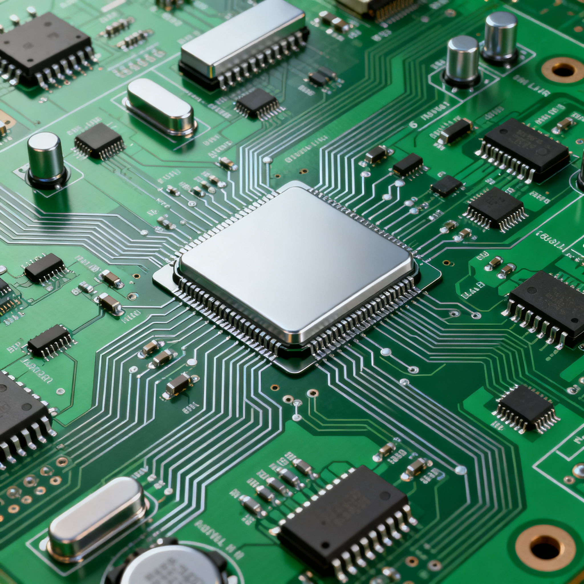
A 6-layer PCB is a versatile platform that offers enhanced electrical performance and improved signal integrity compared to simpler boards. This architecture typically includes two signal layers, two power planes, and two ground planes, allowing for efficient power distribution and noise reduction. The design principles for such boards revolve around minimizing electromagnetic interference (EMI), optimizing thermal management, and ensuring reliable interconnections. Key concepts include layer stackup design, trace routing, and impedance control, all crucial for maintaining signal integrity and reducing crosstalk.
Adhering to industry standards, such as those provided by IPC, is essential. These standards offer guidelines on everything from material selection to manufacturing processes, ensuring that the final product meets quality and performance expectations. The integration of advanced components, like integrated circuits (ICs), requires careful attention to datasheets and specifications to ensure compatibility and functionality.
Detailed Specifications
When designing a 6-layer PCB, understanding the core specifications of the components involved is crucial. These specifications guide the selection of appropriate components, ensuring that the board meets the intended performance criteria. Critical specifications include CPU speed, memory capacity, available peripherals, power requirements, and package types. These parameters influence the board's capability to handle complex operations and determine its suitability for various applications.
| Specification | Description | Typical Values |
|---|---|---|
| CPU Speed | Processing speed of the central processing unit | 1.2 GHz - 3.0 GHz |
| Memory | Onboard RAM and storage capacity | 512 MB - 16 GB |
| Peripherals | Available interfaces and connectivity options | USB, SPI, I2C, UART |
| Power | Power consumption and voltage requirements | 3.3V, 5V, 12V |
| Package | Physical package type of components | BGA, QFN, TQFP |
| Temperature Range | Operating temperature range | -40°C to 85°C |
| Dimensions | Physical size of the board | 100mm x 100mm |
| Layer Count | Number of layers in the PCB | 6 layers |
| Signal Integrity | Measures for minimizing signal degradation | Controlled impedance, differential pairs |
| Thermal Management | Techniques for heat dissipation | Heat sinks, thermal vias |
Key Takeaways from the Specifications
The core specifications table highlights the essential parameters that determine the performance and functionality of a 6-layer PCB. CPU speed and memory capacity are critical for processing power and data storage, directly affecting the board's ability to handle complex tasks. Peripherals provide the necessary interfaces for communication with other devices, while power specifications ensure compatibility with power sources. Package types influence the board's design and assembly process, dictating the layout and soldering techniques. Understanding these specifications allows engineers to select components that meet the application's requirements, ensuring optimal performance and reliability.
| Characteristic | Description | Typical Values |
|---|---|---|
| Operating Voltage | Voltage required for operation | 3.3V, 5V |
| Current Consumption | Typical current draw during operation | 500mA - 2A |
| Timing Requirements | Propagation delays and timing constraints | 10ns - 50ns |
| I/O Voltage Levels | Input/output voltage threshold levels | 1.8V, 3.3V |
| ESD Protection | Electrostatic discharge protection measures | 2kV - 8kV |
| Power Dissipation | Heat generated during operation | 1W - 5W |
| Signal Rise Time | Time taken for a signal to rise from low to high | 1ns - 5ns |
| Impedance Control | Maintaining consistent impedance for signal integrity | 50Ω - 75Ω |
| Crosstalk | Unwanted signal coupling between traces | -30dB - -20dB |
| Noise Margin | Allowance for noise in the signal | 0.5V - 1V |
Practical Implications
The electrical characteristics table provides insights into the operational parameters that affect the performance and reliability of a PCB. Operating voltage and current consumption are crucial for ensuring that the board functions within its power budget. Timing requirements and I/O voltage levels influence the board's ability to interface with other systems effectively. ESD protection and power dissipation measures are vital for safeguarding components and maintaining operational stability. Signal rise time, impedance control, and crosstalk considerations are essential for preserving signal integrity, especially in high-speed applications. Understanding these characteristics enables engineers to design robust, reliable, and efficient PCBs.
| Application | Configuration | Benefits |
|---|---|---|
| Consumer Electronics | High-density interconnects | Compact size, enhanced performance |
| Industrial Automation | Robust power management | Reliability, long lifecycle |
| Telecommunications | High-frequency signal routing | Improved signal integrity, reduced EMI |
| Automotive Systems | Thermal management solutions | Heat dissipation, operational stability |
| Medical Devices | Precision signal processing | Accuracy, safety compliance |
| IoT Devices | Low power consumption | Extended battery life, wireless connectivity |
| Military Applications | Ruggedized design | Durability, environmental resistance |
Application Guidelines
The application comparison table illustrates the diverse use cases for 6-layer PCBs, highlighting the configurations and benefits specific to each application. In consumer electronics, high-density interconnects enable compact designs with enhanced performance. Industrial automation benefits from robust power management, ensuring reliability and longevity. Telecommunications applications require high-frequency signal routing to maintain signal integrity and reduce EMI. Automotive systems demand effective thermal management to ensure operational stability. Medical devices prioritize precision signal processing for accuracy and safety compliance. IoT devices focus on low power consumption to extend battery life and enable wireless connectivity. Military applications require ruggedized designs for durability and environmental resistance.
Design Considerations
Designing a 6-layer PCB involves several critical considerations to ensure optimal performance and manufacturability. Key factors include layer stackup, trace routing, and via placement. The layer stackup should be carefully planned to minimize EMI and ensure efficient power distribution. Signal layers should be sandwiched between power and ground planes to reduce crosstalk and improve signal integrity. Trace routing requires careful attention to detail, with controlled impedance paths for high-speed signals and differential pairs for critical lines.
Thermal management is another crucial aspect, as high-performance components can generate significant heat. Techniques such as thermal vias, heat sinks, and copper pours help dissipate heat and maintain temperature stability. Component placement should consider both electrical and thermal constraints, ensuring that sensitive components are adequately shielded from heat sources.
Compliance with IPC standards, such as IPC-2221 for general design and IPC-A-610 for assembly quality, is essential for ensuring that the PCB meets industry requirements. These standards provide guidelines for everything from material selection to manufacturing processes, ensuring that the final product is reliable and high-performing.
Step-by-Step Implementation
- Define the board requirements: Determine the functional and performance requirements of the PCB, considering the intended application and environmental conditions.
- Select components: Choose components based on the core specifications and electrical characteristics, ensuring compatibility and performance.
- Design the layer stackup: Plan the layer arrangement to optimize signal integrity, power distribution, and EMI reduction.
- Route traces: Carefully route traces, considering impedance control, differential pairs, and signal integrity. Use appropriate design tools to simulate and verify the layout.
- Implement thermal management: Design thermal solutions such as heat sinks, thermal vias, and copper pours to manage heat dissipation effectively.
- Conduct design reviews: Perform thorough design reviews and simulations to identify and resolve potential issues before fabrication.
- Fabricate the PCB: Work with a reputable manufacturer, such as PCBWay or Nova PCBA, to fabricate the board according to the design specifications.
- Test and validate: Conduct comprehensive testing to validate the board's performance, reliability, and compliance with industry standards.
Common Issues & Solutions
- Issue: Signal Integrity Problems
- Solution: Implement controlled impedance routing and use differential pairs for high-speed signals to minimize signal degradation.
- Issue: Thermal Management Challenges
- Solution: Use thermal vias, heat sinks, and copper pours to effectively dissipate heat and maintain temperature stability.
- Issue: EMI Interference
- Solution: Optimize layer stackup and use ground planes to shield sensitive signals from electromagnetic interference.
- Issue: Power Distribution Inefficiencies
- Solution: Design robust power planes and use decoupling capacitors to ensure stable power distribution across the board.
- Issue: Component Placement Constraints
- Solution: Carefully plan component placement to balance electrical and thermal requirements, avoiding overcrowding and ensuring adequate spacing.
Applications & Use Cases
6-layer PCBs find applications across various industries due to their versatility and performance advantages. In consumer electronics, they enable compact and high-performance devices such as smartphones and tablets. Industrial automation systems benefit from their reliability and robust power management capabilities. Telecommunications infrastructure relies on their ability to handle high-frequency signals with minimal interference. Automotive systems use them for advanced driver-assistance systems (ADAS) and infotainment units, where thermal management and signal integrity are critical. In medical devices, precision signal processing ensures accuracy and compliance with safety standards. IoT devices leverage their low power consumption and wireless connectivity features.
Selection & Sourcing Guide
When selecting components for a 6-layer PCB, consider factors such as performance requirements, environmental conditions, and budget constraints. Use reliable sources like IC Online for sourcing components, ensuring that they meet the necessary specifications and quality standards. Collaborating with reputable manufacturers and assembly services, such as PCBWay and Nova PCBA, can streamline the production process and ensure high-quality results.
FAQ
- Q: What are the main advantages of a 6-layer PCB?
- A: Enhanced signal integrity, reduced EMI, improved power distribution, and better thermal management.
- Q: How does layer stackup affect PCB performance?
- A: Proper stackup design minimizes crosstalk, optimizes power distribution, and reduces electromagnetic interference.
- Q: What is impedance control, and why is it important?
- A: Impedance control ensures consistent signal transmission, crucial for high-speed applications to prevent signal degradation.
- Q: How do I manage heat dissipation in a 6-layer PCB?
- A: Use thermal vias, heat sinks, and copper pours to effectively dissipate heat and maintain temperature stability.
- Q: What standards should I follow for PCB design?
- A: Adhere to IPC standards like IPC-2221 for design and IPC-A-610 for assembly quality to ensure reliability and compliance.
- Q: How can I prevent crosstalk in my PCB design?
- A: Use ground planes, maintain adequate spacing between traces, and implement differential pairs for critical signals.
- Q: What are the common issues faced in PCB manufacturing?
- A: Signal integrity problems, thermal management challenges, and EMI interference are common issues that require careful design considerations.
Conclusion
Designing a 6-layer multi-functional PCB requires careful consideration of various factors, including core specifications, electrical characteristics, and application requirements. Adhering to industry standards and leveraging advanced design techniques ensures optimal performance, reliability, and manufacturability. By understanding the critical considerations in PCB layout design, engineers can create robust and efficient boards that meet the demands of modern electronic applications.