PCB Layout Design Rules: A Step-by-Step Guide for Efficient Component Placement
PCB Layout Design Rules: A Step-by-Step Guide for Efficient Component Placement table { border-collapse: collapse; width: 100%; margin: 20px 0; } th, td { border: 1px solid #000; padding: 8px; text-al...
Introduction
In the rapidly evolving world of electronics, efficient PCB layout is critical for the optimal performance of electronic devices. Proper component placement not only ensures functionality but also impacts the manufacturability and reliability of the product. This article delves into the essential aspects of PCB layout design, focusing on the selection and placement of integrated circuit (IC) components. By adhering to industry standards and best practices, engineers can enhance the performance and longevity of their designs.
Technical Overview
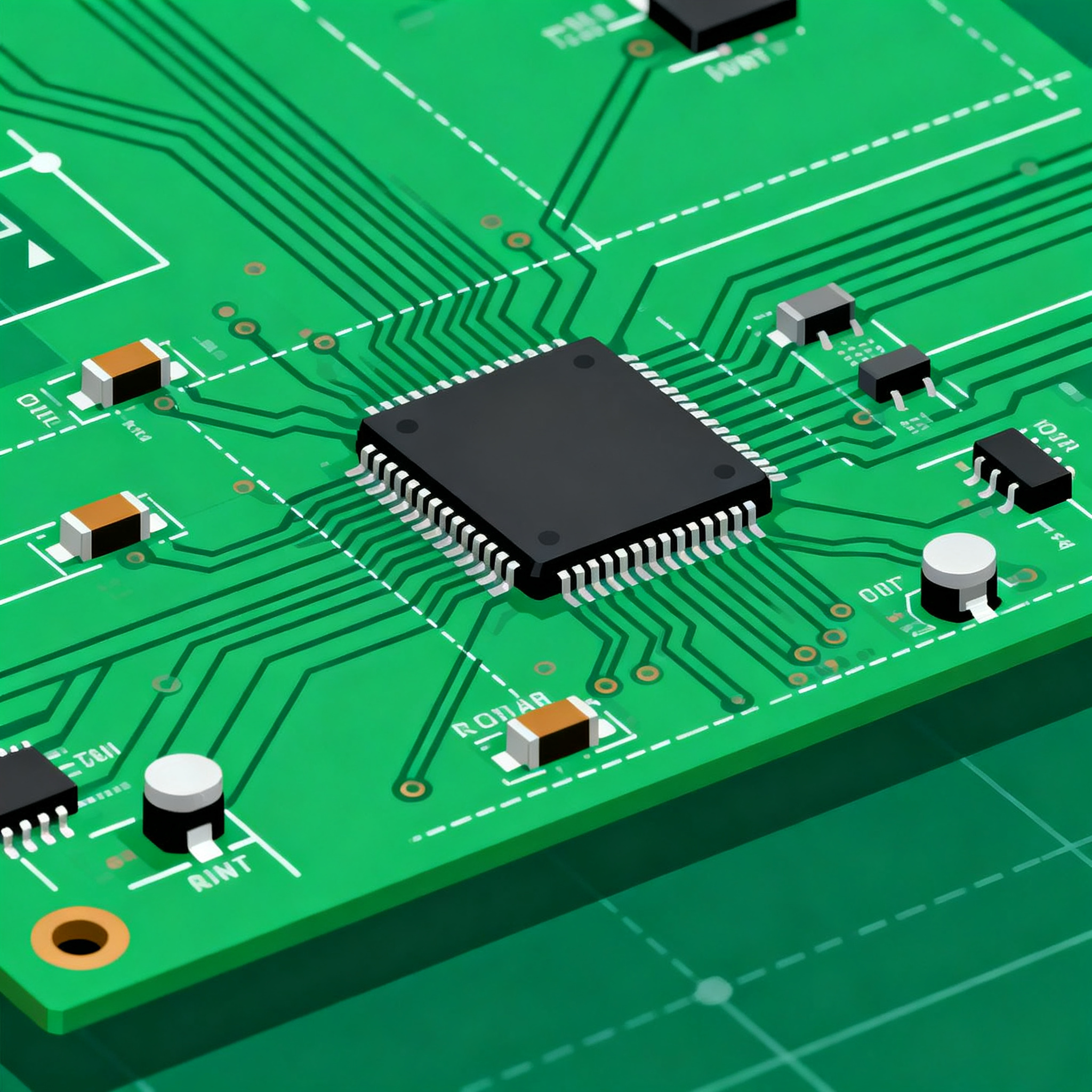
PCB layout design encompasses the strategic arrangement of components and routing of electrical connections on a printed circuit board. This process is guided by various design rules and standards, such as those provided by the IPC. The layout must account for electrical, thermal, and mechanical considerations to ensure the circuit's efficiency. Key principles include minimizing signal interference, optimizing power distribution, and ensuring adequate thermal management. The choice of components, guided by datasheets and specifications, plays a crucial role in achieving these objectives.
Detailed Specifications
Understanding component specifications is vital for effective PCB design. Specifications provide detailed information about the electrical and physical characteristics of components, guiding their selection and placement. Key specifications include CPU speed, memory capacity, peripheral interfaces, power requirements, and package type. These parameters influence the board's performance and compatibility with other components.
| Specification | Details | Notes |
|---|---|---|
| CPU Speed | 1.8 GHz | Optimal for moderate-performance applications |
| Memory | 256 MB RAM | Sufficient for basic operations |
| Peripherals | USB, I2C, SPI | Versatile connectivity options |
| Power Supply | 3.3V | Standard low-power applications |
| Package Type | LQFP | Low-profile, easy to solder |
| Operating Temperature | -40°C to 85°C | Suitable for industrial environments |
| Storage Temperature | -55°C to 150°C | Long-term reliability |
| Dimensions | 10x10 mm | Compact design |
| Weight | 1.5 grams | Lightweight for portable devices |
| MTBF | 50,000 hours | High reliability |
Key Takeaways from the Specifications
The specifications table provides critical insights into the component's capabilities and limitations. For instance, the CPU speed of 1.8 GHz is adequate for applications requiring moderate processing power. The LQFP package type is advantageous for designs needing a low-profile component, making it easier to solder and integrate into compact layouts. Understanding these specifications allows designers to make informed decisions about component selection and placement, ensuring compatibility and performance alignment with the intended application.
| Characteristic | Value | Remarks |
|---|---|---|
| Operating Voltage | 3.3V | Standard for many digital ICs |
| Maximum Current | 500 mA | Ensure adequate power supply |
| Input Impedance | 10 kΩ | High input impedance for minimal loading |
| Output Impedance | 50 Ω | Standard for signal integrity |
| Propagation Delay | 5 ns | Low delay for high-speed applications |
| Rise Time | 2 ns | Fast rise time for sharp signal edges |
| Fall Time | 2 ns | Consistent with rise time |
| Power Dissipation | 1.5 W | Consider heat management |
| ESD Protection | 2 kV | Basic protection level |
| Noise Margin | 0.5V | Ensures reliable operation |
Practical Implications
The electrical characteristics outlined in the table highlight the component's operational limits and performance metrics. For example, the operating voltage of 3.3V is typical for many digital circuits, ensuring compatibility with a wide range of devices. The maximum current of 500 mA necessitates a robust power supply to prevent voltage drops. Additionally, parameters like propagation delay and rise time are crucial for applications requiring high-speed data transmission, impacting the overall circuit speed and reliability.
| Use Case | Configuration | Benefits |
|---|---|---|
| Consumer Electronics | Standard IC | Cost-effective, widely available |
| Industrial Automation | Ruggedized IC | Enhanced durability and temperature range |
| Automotive Applications | Automotive-grade IC | Meets stringent automotive standards |
| Wearable Devices | Low-power IC | Extended battery life |
| IoT Devices | Wireless-capable IC | Seamless connectivity options |
| Medical Devices | Biocompatible IC | Safe for human contact |
Application Guidelines
The application comparison table illustrates how different configurations of ICs cater to specific industry needs. For instance, automotive-grade ICs are designed to meet rigorous automotive standards, ensuring safety and reliability in harsh conditions. Wearable devices benefit from low-power ICs, which prolong battery life and enhance user experience. By selecting the appropriate configuration, designers can optimize their designs for targeted applications, ensuring performance and compliance with industry-specific requirements.
Design Considerations
When embarking on PCB layout design, several practical guidelines can ensure the success of your project. Firstly, consider the trace width and spacing, which are critical for handling current and preventing signal interference. Adhering to IPC standards, such as IPC-2221 for generic PCB design, can provide a solid foundation for these parameters. Additionally, pay attention to thermal management, especially for high-power components, by incorporating thermal vias and heat sinks where necessary.
Signal integrity is another crucial aspect; ensure that high-speed signals are routed with minimal discontinuities and avoid running them parallel to power traces to prevent crosstalk. Utilize differential pairs for high-speed data lines to maintain signal integrity and reduce electromagnetic interference (EMI).
Component placement should prioritize minimizing signal path lengths and maintaining a logical flow of signals across the board. This reduces latency and improves overall circuit performance. Furthermore, consider the board's manufacturing constraints, such as the minimum drill size and layer count, to ensure that the design is manufacturable within budget.
Finally, validate your design with simulation tools to detect potential issues before fabrication. Tools like SPICE can simulate circuit behavior, allowing you to make adjustments early in the design process, saving time and resources.
Step-by-Step Implementation
- Define Design Requirements: Start by outlining the specifications and constraints of your project, including electrical, mechanical, and environmental factors.
- Select Components: Choose components based on their datasheets, ensuring they meet the performance and compatibility criteria for your design.
- Develop Schematic Diagram: Create a detailed schematic that accurately represents the circuit and its connections, serving as a blueprint for the layout.
- Design PCB Layout: Begin placing components on the PCB, following the guidelines for optimal placement and routing. Ensure adequate spacing and alignment.
- Route Traces: Carefully route electrical traces, prioritizing signal integrity and minimizing trace length. Use vias and layers effectively to manage complex connections.
- Perform Design Rule Check (DRC): Use PCB design software to run a DRC, identifying any violations of design rules or potential issues.
- Prototype and Test: Fabricate a prototype of the PCB and conduct thorough testing to validate performance and identify any necessary adjustments.
- Finalize Design: Implement any changes based on prototype testing and prepare the final design for production, ensuring all documentation is complete.
Common Issues & Solutions
- Signal Crosstalk: Use differential pairs and increase trace spacing to reduce interference.
- Thermal Overheating: Add thermal vias and consider using a thicker copper layer for heat dissipation.
- Power Integrity Issues: Implement a robust power distribution network with adequate decoupling capacitors.
- EMI Problems: Utilize shielding techniques and avoid long parallel traces to minimize EMI.
- Manufacturing Defects: Adhere to manufacturing guidelines and conduct thorough inspections to catch defects early.
- Component Placement Errors: Follow a logical placement strategy, prioritizing critical components and minimizing signal path lengths.
Applications & Use Cases
PCB layout design principles are applicable across various industries. In consumer electronics, efficient component placement enhances device performance and reduces costs. The automotive industry relies on robust PCB designs to meet safety and reliability standards. IoT and wearable devices benefit from compact and power-efficient layouts, extending battery life and improving user experience. By understanding the unique requirements of each application, designers can tailor their PCB layouts to meet specific performance and regulatory demands.
Selection & Sourcing Guide
Choosing the right components is crucial for successful PCB design. Utilize online resources like IC Online to compare specifications, availability, and pricing. Ensure that selected components meet the required standards and are compatible with your design. Consider factors like lead time and supplier reliability when sourcing components to avoid delays in production.
FAQ
- What are the key factors in component placement? Key factors include minimizing signal path lengths, ensuring thermal management, and adhering to design rules for spacing and alignment.
- How can I reduce EMI in my PCB design? Use shielding techniques, maintain adequate trace spacing, and avoid parallel routing of sensitive signals.
- What tools can help with PCB design? Software like Altium Designer, Eagle, and KiCad offer comprehensive features for schematic capture and PCB layout.
- How do I ensure my design is manufacturable? Follow IPC standards, consider manufacturing constraints, and run design rule checks to validate your layout.
- What is the importance of thermal management? Effective thermal management prevents overheating, ensuring component reliability and performance.
- How do I select the right IC for my application? Review datasheets and specifications to ensure compatibility with your design's requirements and performance criteria.
- What is a design rule check (DRC)? A DRC is an automated process that checks the PCB layout against predefined design rules to identify potential issues.
- What should I consider when routing traces? Prioritize signal integrity, minimize trace lengths, and use appropriate widths to handle current without overheating.
- How can I ensure signal integrity in high-speed designs? Utilize differential pairs, maintain consistent impedance, and avoid discontinuities in trace routing.
- What are the benefits of using simulation tools? Simulation tools allow you to validate circuit behavior and detect issues before fabrication, saving time and resources.
Conclusion
Efficient PCB layout design is essential for the performance and reliability of electronic devices. By understanding and applying key design principles, engineers can optimize component placement, ensure signal integrity, and meet industry standards. This comprehensive guide provides the knowledge and tools needed to navigate the complexities of PCB layout, ultimately leading to successful and manufacturable designs.