PCB Layout Design Rules: A Practical Guide to Creating Effective Multi-Layer Boards
PCB Layout Design Rules: A Practical Guide to Creating Effective Multi-Layer Boards body { font-family: Arial, sans-serif; line-height: 1.6; margin: 0; padding: 20px; } h2 { margin-top: 40px; color: #...
Introduction
In the fast-evolving world of electronics, designing an effective multi-layer printed circuit board (PCB) is crucial for ensuring robust performance and functionality. With the increasing complexity of modern electronic devices, understanding PCB layout design rules is essential for engineers and designers. This guide aims to provide a comprehensive overview of the key aspects of PCB layout design, focusing specifically on component specifications, datasheets, selection criteria, and application circuits.
Technical Overview
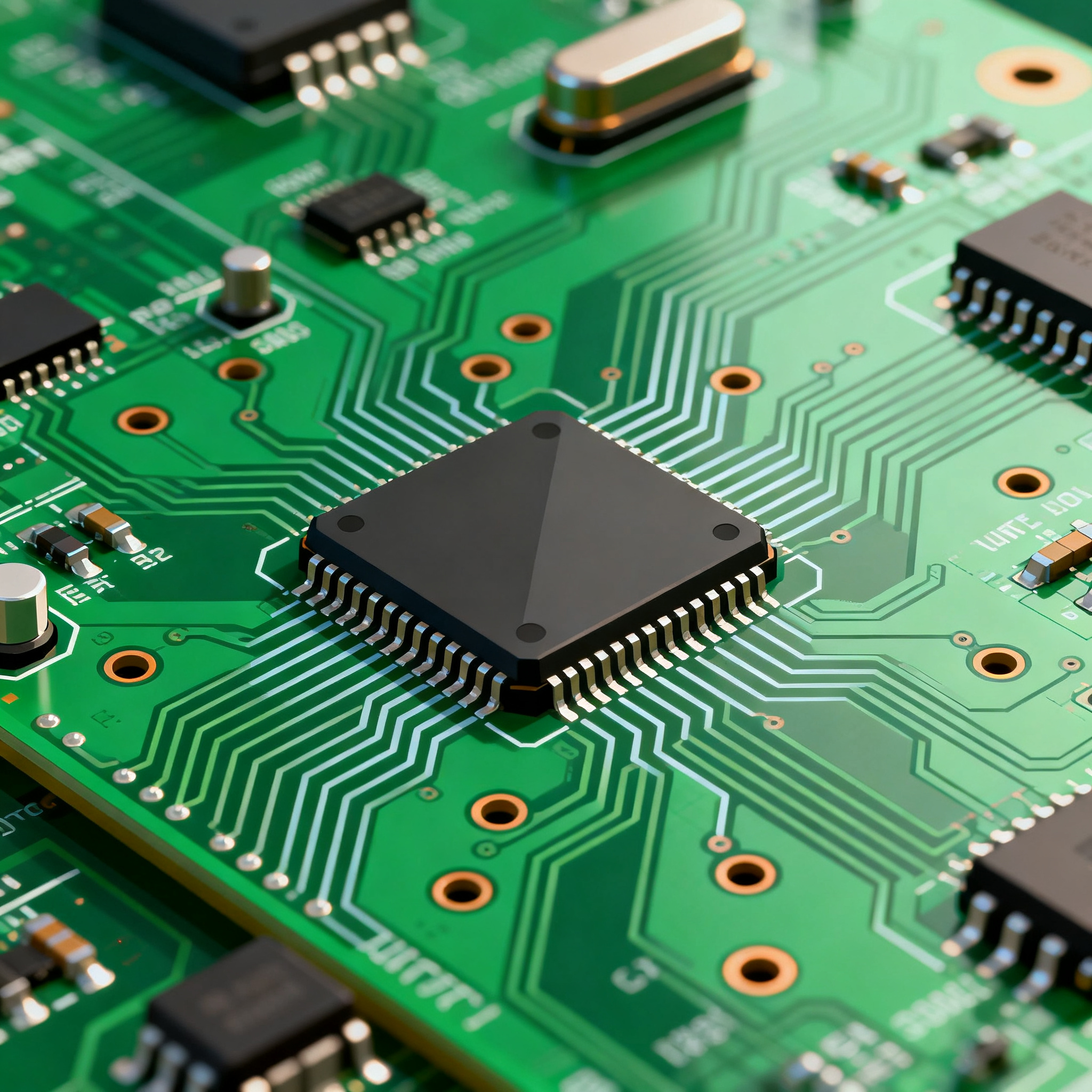
PCB layout design is the process of creating the physical layout of electronic components on a board. It involves arranging components and routing traces to ensure electrical connectivity and performance. Multi-layer boards are commonly used in complex applications where space is limited, and signal integrity is critical. The core concepts of PCB layout design include understanding the architecture of multi-layer boards, the principles of signal routing, and the importance of adhering to industry standards such as those from the IPC. Proper design ensures that the board can be manufactured efficiently and functions reliably in its intended application.
Detailed Specifications
When designing a PCB, understanding the specifications of the components you are working with is essential. This includes knowing the CPU speed, memory capacity, available peripherals, power requirements, and the package type of the integrated circuits (ICs) you intend to use. These specifications influence the board's overall performance and dictate the design constraints. Below is a table outlining core specifications for a typical IC chip used in multi-layer PCB designs.
| Specification | Details | Notes |
|---|---|---|
| CPU Speed | 1.5 GHz | High-performance applications |
| Memory | 4 GB DDR4 | Supports high data throughput |
| Peripherals | USB, SPI, I2C | Versatile connectivity options |
| Power Supply | 5V DC | Standard power requirement |
| Package | LQFP-64 | Low-profile quad flat package |
| Operating Temperature | -40°C to 85°C | Suitable for industrial environments |
| Storage Temperature | -55°C to 125°C | Extended storage capability |
| Pin Count | 64 | High integration capability |
| Dimensions | 10mm x 10mm | Compact size |
| Weight | 2 grams | Lightweight |
Key Takeaways from the Specifications
The specifications outlined in the table highlight the critical attributes of an IC used in multi-layer PCB designs. The CPU speed and memory capacity are crucial for determining the processing power and data handling capabilities of the board. Peripherals such as USB, SPI, and I2C offer diverse connectivity options, making the board adaptable for various applications. The power supply requirement of 5V DC is standard, ensuring compatibility with common power sources. The package type and dimensions are important for determining the physical layout and space optimization on the PCB. Understanding these specifications allows designers to make informed decisions about component selection and board design.
| Electrical Characteristic | Value | Notes |
|---|---|---|
| Operating Voltage | 3.3V | Standard for digital circuits |
| Maximum Current | 500 mA | Ensure adequate power supply |
| Input Voltage Range | 2.7V - 3.6V | Allows for voltage variation |
| Output Current | 100 mA per I/O | Check for total current draw |
| Clock Frequency | 100 MHz | Important for timing-sensitive applications |
| Rise Time | 5 ns | Affects signal integrity |
| Fall Time | 5 ns | Affects signal integrity |
| Input Capacitance | 10 pF | Influences signal speed |
| Output Capacitance | 12 pF | Influences signal speed |
| Power Dissipation | 1 W | Consider thermal management |
| Impedance | 50 ohms | Standard for signal traces |
| Junction Temperature | 125°C | Max operating temperature |
Practical Implications
The electrical characteristics table provides essential information for ensuring the PCB operates within safe and efficient parameters. Understanding the operating voltage and current limits is crucial for designing power distribution networks and selecting appropriate components. The clock frequency and rise/fall times are vital for timing-sensitive applications, affecting signal integrity and overall performance. Power dissipation and impedance values help guide thermal management and trace routing decisions. By comprehensively understanding these electrical characteristics, designers can optimize the PCB layout for performance and reliability.
| Application | Configuration | Benefits |
|---|---|---|
| Embedded Systems | Single-board, low power | Compact design, energy-efficient |
| Consumer Electronics | Multi-layer, high performance | Enhanced functionality, user experience |
| Industrial Automation | Rugged, high temperature | Reliability in harsh conditions |
| Networking Equipment | High-speed, low latency | Improved data throughput |
| Automotive Systems | Robust, EMI shielding | Enhanced safety, performance |
| Medical Devices | Miniaturized, low noise | Precision, reliability |
| Telecommunications | High-frequency, multi-channel | Scalability, efficiency |
| Aerospace Applications | Lightweight, radiation-hardened | Durability, performance in space |
Application Guidelines
The application comparison table showcases the versatility of multi-layer PCBs across various industries. Each configuration is tailored to meet the specific demands of its application. For instance, embedded systems benefit from a compact and energy-efficient design, while consumer electronics prioritize high performance and enhanced user experience. Industrial automation requires rugged and reliable solutions to withstand harsh environments. By understanding these application-specific configurations, designers can select the appropriate PCB layout and components to meet the functional and environmental requirements of their projects.
Design Considerations
Designing a multi-layer PCB involves several critical considerations to ensure optimal performance and manufacturability. Signal integrity is paramount, requiring careful trace routing and impedance control. Ground planes and power distribution networks must be strategically placed to minimize electromagnetic interference (EMI) and ensure stable power delivery. Thermal management is another crucial aspect, as excessive heat can impact component reliability and performance. Designers should consider using thermal vias, heat sinks, and appropriate copper thickness to manage heat dissipation effectively.
Component placement is also vital for maintaining signal integrity and reducing noise. High-frequency components should be placed close to their respective connectors to minimize trace length and potential signal degradation. Additionally, designers must adhere to industry standards, such as IPC-2221, to ensure the board meets quality and reliability requirements. Collaboration with PCB manufacturers early in the design process can help address potential manufacturing challenges and optimize the design for cost-effective production.
Step-by-Step Implementation
- Define Requirements: Start by defining the project's requirements, including functionality, performance, and environmental conditions.
- Select Components: Choose components based on the defined requirements, considering specifications, availability, and cost.
- Create Schematic: Develop a schematic diagram using design software to outline the electrical connections and component relationships.
- Design PCB Layout: Use PCB design software to create the physical layout, placing components and routing traces based on the schematic.
- Conduct DRC: Perform a Design Rule Check (DRC) to identify and resolve any layout issues before manufacturing.
- Prototype and Test: Fabricate a prototype board and conduct thorough testing to verify functionality and performance.
- Optimize Design: Analyze test results and make necessary design adjustments to optimize performance and manufacturability.
- Finalize Design: Finalize the design and prepare the necessary documentation for manufacturing, including Gerber files and assembly drawings.
Common Issues & Solutions
- Signal Integrity Issues: Use controlled impedance traces and proper termination to minimize signal reflections and crosstalk.
- EMI Problems: Incorporate ground planes and EMI shielding to reduce electromagnetic interference and improve signal quality.
- Thermal Management Challenges: Use thermal vias, heat sinks, and appropriate copper thickness to manage heat dissipation effectively.
- Component Placement Errors: Ensure critical components are placed close to connectors and consider signal path lengths for optimal performance.
- Manufacturing Defects: Collaborate with PCB manufacturers to address potential fabrication challenges and improve yield.
- Power Distribution Issues: Design robust power distribution networks with adequate decoupling capacitors to ensure stable power delivery.
Applications & Use Cases
Multi-layer PCBs find applications in various industries, each with unique requirements and challenges. In consumer electronics, multi-layer boards enable compact and feature-rich designs, enhancing user experience. In the automotive industry, robust and reliable PCBs are essential for safety and performance in harsh environments. Medical devices benefit from miniaturized and low-noise PCBs, ensuring precision and reliability. Networking equipment relies on high-speed, low-latency designs for improved data throughput, while aerospace applications demand lightweight and radiation-hardened solutions for durability and performance in space.
Selection & Sourcing Guide
When selecting and sourcing components for your PCB design, consider factors such as specifications, availability, and cost. Utilize resources like IC Online to find a wide range of components that meet your design requirements. Collaborate with suppliers to ensure timely delivery and access to the latest technologies. Additionally, consider working with PCB manufacturers who offer flexible minimum order quantities (MOQ) and fast turnaround times to meet project deadlines.
FAQ
- What are the benefits of using multi-layer PCBs? Multi-layer PCBs offer increased design flexibility, improved signal integrity, and compact form factors, making them ideal for complex applications.
- How do I ensure signal integrity in my PCB design? Use controlled impedance traces, proper termination, and minimize trace lengths to reduce signal reflections and crosstalk.
- What are common challenges in thermal management? Managing heat dissipation is crucial; use thermal vias, heat sinks, and appropriate copper thickness to address thermal challenges.
- How can I reduce EMI in my PCB design? Incorporate ground planes and EMI shielding, and use differential pairs to minimize electromagnetic interference.
- What should I consider when selecting components? Consider specifications, availability, cost, and compatibility with your design requirements when selecting components.
- How do I perform a Design Rule Check (DRC)? Use PCB design software to conduct a DRC, which checks for layout issues such as trace widths, clearances, and component placement.
- What are the key considerations for component placement? Place critical components close to connectors, minimize signal path lengths, and consider thermal management in your layout.
- How can I improve the manufacturability of my PCB design? Collaborate with PCB manufacturers early in the design process to address potential fabrication challenges and optimize the design.
- What is the importance of power distribution networks? Robust power distribution networks with adequate decoupling capacitors ensure stable power delivery to all components.
- How do I optimize my PCB design for cost-effective production? Optimize component selection, layout, and routing to minimize material usage and manufacturing complexity, reducing overall production costs.
Conclusion
Understanding PCB layout design rules is essential for creating effective multi-layer boards that meet performance, reliability, and manufacturability requirements. By comprehensively analyzing component specifications, electrical characteristics, and application configurations, designers can make informed decisions that optimize their designs. Collaboration with PCB manufacturers and adherence to industry standards further enhances the quality and success of the final product. With this guide, you are equipped with the knowledge to tackle the challenges of multi-layer PCB design and achieve outstanding results.