pcb layout design rules
PCB Layout Design Rules Introduction The world of electronics design is continuously evolving, and Printed Circuit Boards (PCBs) are at the heart of this technological advancement. Whether in consumer...
Introduction
The world of electronics design is continuously evolving, and Printed Circuit Boards (PCBs) are at the heart of this technological advancement. Whether in consumer electronics, industrial systems, or cutting-edge telecommunications, PCBs form the backbone of these devices by providing a platform for electronic components and circuits. Understanding PCB layout design rules is crucial for engineers to ensure their designs are manufacturable, reliable, and cost-effective. This article delves into the core aspects of PCB design, focusing on circuit topology, component calculations, performance analysis, and design trade-offs to guide engineers in creating optimized PCB layouts.
Technical Overview
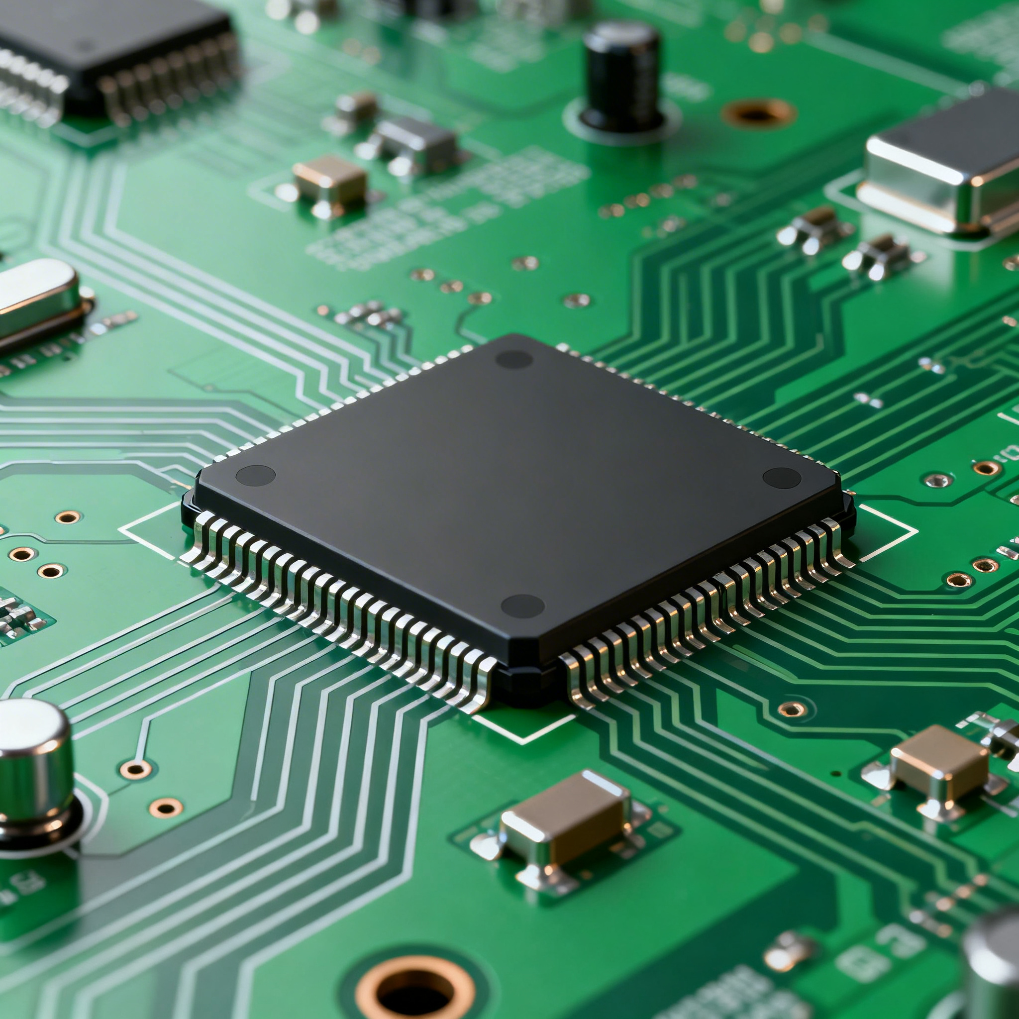
PCB layout design involves several core concepts such as circuit topology, signal integrity, thermal management, and manufacturability. Circuit topology refers to the arrangement of components and their interconnections on the PCB. It is essential to understand the principles of signal routing, grounding, and power distribution to minimize electromagnetic interference (EMI) and signal loss. Additionally, thermal management is vital to prevent overheating, which can degrade performance and reliability.
Adhering to IPC standards, such as IPC-A-610 and IPC-2221, ensures that designs meet industry quality benchmarks. These standards provide guidelines on trace widths, spacing, and material selection, which are critical for robust design. Furthermore, leveraging resources from manufacturers like PCBWay and Nova PCBA can aid in understanding fabrication constraints and assembly processes, ensuring that the design is not only functional but also manufacturable.
Detailed Specifications
When designing a PCB, several specifications need to be meticulously calculated and adhered to. These include component values, trace dimensions, power requirements, and thermal considerations. Proper calculations ensure that the PCB will perform as intended under various operating conditions, and help in avoiding costly redesigns and manufacturing issues.
| Parameter | Value | Formula/Calculation |
|---|---|---|
| Resistor Value | 1kΩ | V=IR, where V = 5V, I = 5mA |
| Capacitor Value | 10uF | C=Q/V, Q=100uC, V=10V |
| Inductor Value | 10mH | VL=L(di/dt), di/dt=1A/ms |
| Trace Width | 0.25mm | Based on IPC-2221 for 1A current |
| Trace Spacing | 0.2mm | Based on IPC-2221 for 50V |
| Power Dissipation | 0.5W | P=IV, I=100mA, V=5V |
| Thermal Resistance | 50°C/W | Based on material properties |
| Signal Frequency | 1GHz | f=1/T, T=1ns |
| Dielectric Constant | 4.5 | Based on FR4 material |
| Layer Count | 4 layers | Based on design complexity |
Key Takeaways from the Specifications
The specifications outlined in the table above are critical for ensuring the PCB functions correctly and reliably. For instance, selecting appropriate resistor and capacitor values is vital for achieving desired signal characteristics and filtering effects. The trace width and spacing are determined based on current carrying capacity and voltage levels, adhering to IPC standards to avoid issues like trace overheating and short circuits. Additionally, understanding thermal resistance and power dissipation helps in managing heat within the PCB, thereby enhancing the longevity and performance of the device. These parameters form the foundation of a robust PCB design, ensuring that the circuit can handle the intended electrical and thermal loads.
| Performance Metric | Value | Analysis |
|---|---|---|
| Gain | 20 dB | Amplifier stage performance |
| Bandwidth | 500 MHz | Suitable for RF applications |
| Noise Figure | 3 dB | Low noise design |
| Power Consumption | 2 W | Efficient power management |
| Signal Integrity | High | Minimal signal loss |
| Thermal Stability | Stable up to 85°C | Ensures reliability |
| Impedance Matching | 50Ω | Optimal signal transfer |
| EMI Susceptibility | Low | Good shielding practices |
| Latency | 5 ns | Fast signal processing |
Practical Implications
The performance metrics provided in the table are essential for evaluating the effectiveness of a PCB design. A gain of 20 dB indicates a robust amplification stage, which is crucial for applications requiring significant signal boosting. The bandwidth of 500 MHz suggests suitability for high-frequency RF applications, while a noise figure of 3 dB highlights the design's low noise characteristics. Power consumption of 2 W reflects efficient energy use, critical in battery-powered devices. Signal integrity, thermal stability, and EMI susceptibility are key factors affecting the reliability and efficiency of the PCB in real-world conditions. Understanding these metrics allows engineers to optimize their designs for specific applications, ensuring high performance and reliability.
| Configuration | Pros | Cons |
|---|---|---|
| Single-layer PCB | Cost-effective, simple design | Limited routing space |
| Double-layer PCB | Increased routing options | Higher cost than single-layer |
| Multi-layer PCB | Compact design, high performance | Complex manufacturing |
| Flexible PCB | Versatile, lightweight | Higher material cost |
| Rigid-flex PCB | Combines rigidity and flexibility | Design complexity |
| Through-hole Technology | Strong mechanical bonds | Larger PCB size |
| Surface-mount Technology | Compact, supports high density | Requires precise placement |
Application Guidelines
Choosing the right configuration for a PCB design involves understanding the trade-offs between different options. Single-layer PCBs are cost-effective and suitable for simple applications, but they offer limited routing space. Double-layer PCBs provide more routing options, making them ideal for slightly more complex designs. Multi-layer PCBs, while offering compact and high-performance solutions, involve complex manufacturing processes. Flexible and rigid-flex PCBs offer versatility and are suitable for applications requiring bending or folding. The choice between through-hole and surface-mount technology depends on the need for mechanical strength versus compact design. Understanding these trade-offs helps in selecting the appropriate configuration that meets the specific requirements of the application while balancing cost and performance.
Design Considerations
When designing a PCB, several considerations must be taken into account to ensure successful implementation. Signal integrity is paramount, requiring careful routing of traces to minimize crosstalk and EMI. Power distribution should be planned to ensure stable voltage supply to all components, often involving the use of power planes and decoupling capacitors. Thermal management is another crucial aspect, necessitating the use of heat sinks, thermal vias, and proper component placement to dissipate heat effectively. Additionally, manufacturability should be considered, with designs adhering to the capabilities and limitations of the chosen fabrication process. Ensuring compliance with industry standards, such as IPC guidelines, is also vital for quality assurance. By addressing these considerations, engineers can create PCB designs that are robust, efficient, and reliable.
Step-by-Step Implementation
Implementing a PCB design involves several detailed steps, each crucial for ensuring a successful outcome:
- Requirement Analysis: Begin by defining the requirements of the PCB, including electrical, mechanical, and environmental specifications. This step involves understanding the application's needs and constraints.
- Schematic Design: Create a schematic diagram that represents the circuit topology, showing all components and their connections. Use CAD software to ensure accuracy and ease of modification.
- Component Selection: Choose components based on the design requirements, considering factors such as availability, cost, and performance. Ensure that selected components meet the necessary specifications.
- PCB Layout Design: Using PCB design software, translate the schematic into a physical layout. Pay attention to trace routing, layer management, and component placement to optimize performance and manufacturability.
- Design Rule Check (DRC): Conduct automated checks to ensure that the design adheres to predefined rules, such as trace width, spacing, and clearances. This step helps identify potential issues before fabrication.
- Prototype Fabrication: Send the design to a PCB manufacturer for prototype fabrication. Choose a manufacturer that meets the design's complexity and quality requirements, such as PCBWay or Nova PCBA.
- Testing and Validation: Once the prototype is fabricated, perform thorough testing to validate the design's performance against the initial requirements. This step may involve electrical, thermal, and mechanical tests.
- Design Iteration: Based on testing results, make necessary adjustments to the design. This iterative process helps refine the PCB for optimal performance and reliability.
Common Issues & Solutions
PCB design and implementation can face several common issues, each with potential solutions:
- Signal Integrity Problems: Issues like crosstalk and signal reflections can be mitigated by careful trace routing, impedance matching, and the use of ground planes.
- Thermal Management Challenges: Overheating can be addressed by using thermal vias, heat sinks, and strategic component placement to enhance heat dissipation.
- EMI Considerations: Minimize electromagnetic interference by using proper shielding, grounding techniques, and maintaining adequate spacing between traces.
- Manufacturability Issues: Ensure the design complies with the manufacturer's capabilities, considering factors like minimum trace width and spacing, and panelization requirements.
- Component Availability: Mitigate supply chain risks by selecting alternative components that meet the same specifications, and maintaining good communication with suppliers.
- Design Rule Violations: Regularly run Design Rule Checks (DRC) during the layout process to catch violations early and avoid costly rework.
Applications & Use Cases
PCBs are used in a wide range of applications across various industries. In consumer electronics, they are found in smartphones, tablets, and TVs, where compact and efficient design is crucial. In the automotive industry, PCBs are used in engine control units, infotainment systems, and advanced driver-assistance systems, requiring robust and reliable designs. Industrial applications include automation systems and machinery, where PCBs must withstand harsh environments and ensure high performance. In telecommunications, PCBs are used in networking equipment and communication devices, emphasizing high-frequency performance and signal integrity. These diverse use cases highlight the importance of tailored PCB design to meet specific application needs.
Selection & Sourcing Guide
When selecting and sourcing components for a PCB design, it is crucial to consider factors such as availability, cost, and performance. Utilize resources like IC Online to find reliable suppliers and compare different components. Consider working with manufacturers who offer flexible minimum order quantities and fast turnaround times, such as those found on PCBWay or Nova PCBA. Establishing strong relationships with suppliers can ensure a steady supply chain and minimize the risk of component shortages.
FAQ
- What is the importance of trace width in PCB design? Trace width is crucial for ensuring that the traces can carry the required current without overheating or causing voltage drops.
- How can I minimize EMI in my PCB design? EMI can be minimized by using proper grounding techniques, shielding, and maintaining adequate spacing between traces.
- What should I consider when selecting PCB materials? Consider factors such as thermal conductivity, dielectric constant, and cost when selecting PCB materials.
- How do I ensure signal integrity in high-frequency designs? Ensure signal integrity by using controlled impedance traces, minimizing via usage, and maintaining consistent trace lengths.
- What are the benefits of using multi-layer PCBs? Multi-layer PCBs offer increased routing space, improved signal integrity, and the ability to separate power and ground planes.
- How can I optimize thermal management in my PCB design? Optimize thermal management by using thermal vias, heat sinks, and strategic component placement to enhance heat dissipation.
- What is the role of decoupling capacitors in PCB design? Decoupling capacitors help stabilize the power supply voltage by providing a local energy reservoir for components.
- How do I perform a Design Rule Check (DRC)? Use PCB design software to run automated DRCs, which check for violations of predefined design rules such as trace width, spacing, and clearances.
- What are the advantages of surface-mount technology (SMT)? SMT offers compact design, supports high component density, and is suitable for automated assembly processes.
- How do I choose the right PCB manufacturer? Choose a PCB manufacturer based on their capabilities, quality standards, lead times, and cost-effectiveness, ensuring they can meet your design's requirements.
Conclusion
PCB layout design is a multifaceted discipline that requires careful consideration of various parameters to ensure a successful outcome. By understanding circuit topology, component calculations, performance analysis, and design trade-offs, engineers can create PCBs that meet the demands of modern electronic applications. Adhering to industry standards and leveraging the capabilities of reliable manufacturers can further enhance the quality and reliability of the final product. As technology advances, staying informed about the latest design practices and tools will be essential for engineers to continue delivering innovative and efficient PCB designs.