PCB Layout Best Practices: Step-by-Step Techniques for Optimal Signal Integrity
PCB Layout Best Practices: Step-by-Step Techniques for Optimal Signal Integrity Introduction In the rapidly evolving electronics industry, the design and layout of printed circuit boards (PCBs) are cr...
Introduction
In the rapidly evolving electronics industry, the design and layout of printed circuit boards (PCBs) are critical for ensuring optimal signal integrity and device performance. As technology advances, components become more compact and powerful, requiring intricate PCB designs to support them. This article delves into PCB layout best practices, focusing on component specifications, selection criteria, and application circuits, which are essential for achieving reliable and efficient electronic devices. By adhering to industry standards and leveraging modern design techniques, engineers can enhance the performance and longevity of their products.
Technical Overview
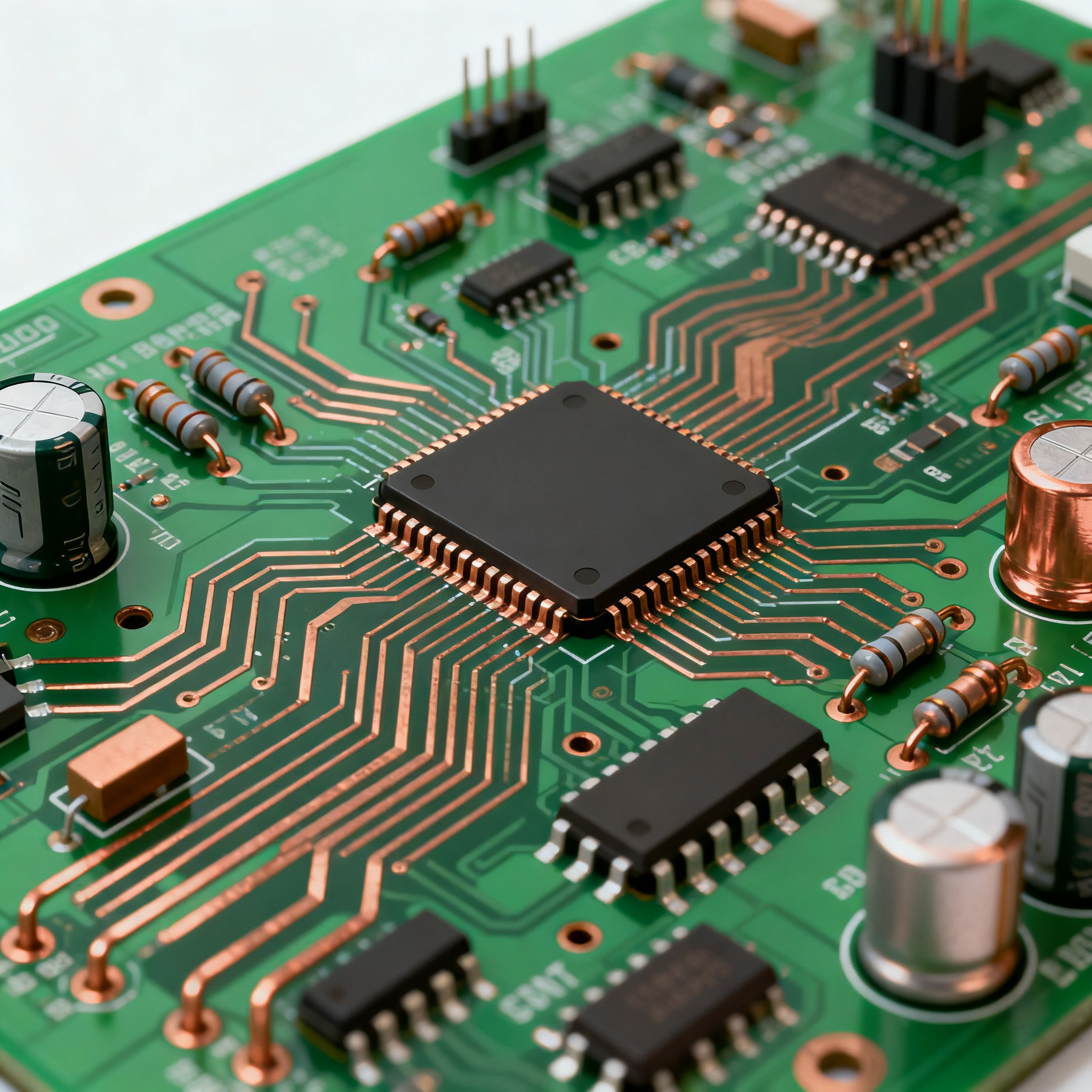
PCB layout is a fundamental aspect of electronics design, influencing signal integrity, power distribution, and thermal management. The architecture of a PCB involves multiple layers that route electrical signals between components like IC chips, resistors, capacitors, and more. Ensuring optimal signal integrity involves minimizing electromagnetic interference (EMI), reducing crosstalk, and maintaining proper impedance matching. Key principles include the use of ground planes, controlled impedance traces, and strategic placement of components to minimize loop areas. Understanding these core concepts is vital for engineers aiming to design high-performance PCBs that meet industry standards such as IPC-2221 and IPC-A-610.
Detailed Specifications
When selecting IC chips for PCB design, several specifications are critical. These include CPU speed, memory capacity, peripheral interfaces, power requirements, and packaging options. Understanding these specifications helps engineers make informed decisions, ensuring compatibility and performance in the final product. The following table outlines core specifications for a typical IC chip used in high-performance applications.
| Specification | Details | Importance |
|---|---|---|
| CPU Speed | 2.5 GHz | Determines processing power |
| Memory | 4 GB DDR4 | Influences multitasking capability |
| Peripherals | USB, HDMI, I2C, SPI | Connectivity options |
| Power Supply | 3.3V - 5V | Voltage range for operation |
| Package Type | QFN, BGA | Physical form factor |
| Temperature Range | -40°C to 85°C | Operational environment |
| Clock Speed | 1.5 GHz | Determines data throughput |
| Pin Count | 64 pins | Number of I/O connections |
| Die Size | 5mm x 5mm | Space on PCB |
| ESD Protection | 2 kV | Prevents electrostatic damage |
| Lifecycle | 5 years | Product longevity |
| Compliance | RoHS, REACH | Environmental standards |
Key Takeaways from the Specifications
The specifications outlined in the table above highlight the critical parameters that influence the selection and integration of IC chips in PCB design. CPU speed and memory directly affect the processing capabilities and efficiency of the device, while peripheral interfaces determine the range of connectivity options available. Power supply specifications ensure compatibility with the existing power infrastructure, and the package type dictates the physical footprint of the component on the PCB. Understanding these factors is crucial for designing robust and efficient electronic systems, as they directly impact performance, reliability, and cost.
| Characteristic | Specification | Importance |
|---|---|---|
| Operating Voltage | 3.3V | Standard logic level |
| Maximum Current | 500 mA | Load capacity |
| Input Voltage Range | 2.7V - 5.5V | Power flexibility |
| Output Current | 20 mA per pin | Driving capability |
| Propagation Delay | 10 ns | Signal timing |
| Input Leakage Current | 1 µA | Minimizes power loss |
| Output Impedance | 50 Ω | Signal integrity |
| ESD Protection | 2 kV | Device safety |
| Thermal Resistance | 30°C/W | Heat dissipation |
| Clock Jitter | 5 ps | Accuracy of timing |
| Noise Margin | 0.4V | Signal reliability |
| Power Dissipation | 1 W | Thermal management |
Practical Implications
The electrical characteristics detailed in the table play a crucial role in ensuring the functionality and reliability of a PCB design. Operating voltage and maximum current specifications are essential for determining the power requirements and ensuring that the design can handle the expected load. Propagation delay and clock jitter are critical for maintaining precise timing and synchronization in high-speed applications. Additionally, thermal resistance and power dissipation metrics are vital for effective thermal management, preventing overheating and ensuring the longevity of the device. Engineers must carefully consider these characteristics to optimize performance and maintain signal integrity throughout the system.
| Application | Configuration | Benefits |
|---|---|---|
| Consumer Electronics | Low-power, compact | Energy efficiency |
| Industrial Automation | Robust, high-temp | Reliability |
| Automotive Systems | High-speed, EMI-resistant | Safety and performance |
| IoT Devices | Wireless, scalable | Connectivity |
| Telecommunications | High bandwidth, low latency | Data throughput |
| Medical Devices | Precision, low-noise | Accuracy |
| Aerospace Systems | Radiation-hardened | Durability |
| Wearable Tech | Miniaturized, flexible | Portability |
Application Guidelines
The application comparison table illustrates the diverse configurations and benefits of PCB designs across various industries. For consumer electronics, low-power and compact configurations are prioritized to enhance energy efficiency and portability. Industrial automation applications require robust designs capable of withstanding high temperatures and harsh environments. Automotive systems demand high-speed, EMI-resistant designs to ensure safety and performance. Each industry has unique requirements, and selecting the appropriate configuration is essential for optimizing functionality and meeting specific application needs. Engineers must evaluate these criteria to ensure their designs are fit for purpose and compliant with industry standards.
Design Considerations
Designing a PCB with optimal signal integrity involves a comprehensive understanding of various factors that influence performance. Engineers must consider trace width and spacing, which affect impedance and signal integrity. Ground planes are essential for reducing EMI and providing a stable reference voltage. Decoupling capacitors should be placed strategically near power pins to minimize voltage fluctuations. Additionally, the use of vias should be minimized to reduce parasitic inductance and capacitance. Component placement is critical for minimizing loop areas and reducing crosstalk. By adhering to these design guidelines, engineers can create PCBs that deliver reliable performance and meet industry standards.
Step-by-Step Implementation
- Define the requirements: Understand the application needs and set design specifications accordingly.
- Select components: Choose IC chips and other components based on performance, cost, and availability.
- Design the schematic: Create a detailed schematic diagram that outlines the electrical connections and component placements.
- Optimize the layout: Arrange components strategically to minimize trace lengths and reduce EMI.
- Route the traces: Use controlled impedance routing techniques to maintain signal integrity and reduce crosstalk.
- Implement power distribution: Design robust power and ground planes to ensure stable voltage levels across the PCB.
- Perform DFM checks: Conduct design for manufacturability (DFM) checks to ensure the PCB can be reliably manufactured.
- Prototype and test: Fabricate a prototype PCB and conduct thorough testing to verify performance and reliability.
Common Issues & Solutions
- Signal Crosstalk: Increase trace spacing and use ground planes to minimize interference.
- EMI Problems: Implement shielding and use differential signaling to reduce EMI susceptibility.
- Power Integrity Issues: Use decoupling capacitors and design robust power distribution networks.
- Thermal Management: Incorporate thermal vias and heat sinks to dissipate excess heat effectively.
- Component Placement: Optimize placement to minimize loop areas and improve signal integrity.
- Manufacturing Defects: Conduct thorough design reviews and DFM checks to prevent defects.
Applications & Use Cases
PCB designs are integral to a wide range of applications, from consumer electronics to aerospace systems. In consumer electronics, PCBs enable compact and efficient designs for smartphones, tablets, and wearables. Industrial applications rely on robust PCBs for automation and control systems. Automotive and aerospace industries demand high-speed, reliable PCBs to ensure safety and performance in critical systems. Medical devices utilize PCBs for precision and accuracy in diagnostics and treatment equipment. Each application presents unique challenges and opportunities, requiring tailored PCB designs to meet specific requirements and performance criteria.
Selection & Sourcing Guide
When selecting IC chips for your PCB design, consider factors such as performance, cost, and availability. Utilize resources like IC Online to compare different components and find the best fit for your application. Evaluate datasheets, application notes, and manufacturer recommendations to ensure compatibility and reliability. Collaborate with suppliers to secure competitive pricing and reliable delivery times, ensuring a smooth production process and timely project completion.
FAQ
- What is signal integrity? Signal integrity refers to the quality and reliability of electrical signals as they pass through a PCB, affecting performance and functionality.
- How can I reduce EMI in my PCB design? Use ground planes, shielded traces, and differential signaling to minimize electromagnetic interference.
- What is the importance of decoupling capacitors? Decoupling capacitors stabilize voltage levels and reduce noise by filtering out high-frequency fluctuations.
- How do I choose the right IC chip for my application? Consider specifications like CPU speed, memory, power requirements, and peripheral interfaces to ensure compatibility and performance.
- What are design for manufacturability (DFM) checks? DFM checks ensure that a PCB design can be reliably manufactured, reducing the risk of defects and production delays.
- Why is thermal management important in PCB design? Effective thermal management prevents overheating, ensuring the reliability and longevity of electronic components.
- What role do ground planes play in PCB design? Ground planes provide a stable reference voltage, reduce EMI, and improve signal integrity by minimizing loop areas.
- How can I improve the signal integrity of high-speed traces? Use controlled impedance routing, minimize trace lengths, and avoid unnecessary vias to maintain signal integrity.
- What are the benefits of using a multi-layer PCB? Multi-layer PCBs allow for more complex designs, better signal integrity, and improved power distribution.
- How can I ensure my PCB design meets industry standards? Adhere to guidelines from standards organizations like IPC and conduct thorough design reviews to ensure compliance.
Conclusion
PCB layout best practices are essential for achieving optimal signal integrity and performance in electronic designs. By understanding component specifications, electrical characteristics, and application requirements, engineers can design robust and reliable PCBs that meet industry standards. From selecting the right components to implementing effective design techniques, a comprehensive approach ensures successful outcomes in a variety of applications. By following the guidelines and insights provided in this article, engineers can enhance their designs and deliver high-quality products that meet the demands of modern technology.