Certainly! Here is a comprehensive article on PCB assembly equipment with the required tables and formatting.
---
Introduction
In the realm of electronics, printed circuit boards (PCBs) are the backbone of virtually every electronic device. As the demand for smaller, faster, and more efficient devices grows, so does the complexity of PCB design and assembly. Understanding PCB layout rules, stackup design, signal integrity, and manufacturing considerations is crucial for engineers looking to create reliable and high-performance circuits. This article delves into these critical aspects, providing a detailed overview and practical guidelines to ensure your PCB designs meet industry standards and perform optimally.
Technical Overview
At the heart of PCB design lies a delicate balance between functionality and manufacturability. The architecture of a PCB involves multiple layers, each serving a specific purpose — from signal routing to power distribution. Signal integrity is paramount, ensuring that signals are transmitted without distortion or interference. This requires careful consideration of trace width, spacing, and via sizes, as well as the selection of appropriate materials. IPC standards play a vital role in guiding these design choices, providing a framework for quality and consistency across the industry. By adhering to these standards and leveraging advanced manufacturing techniques, designers can create PCBs that not only meet but exceed performance expectations.
Detailed Specifications
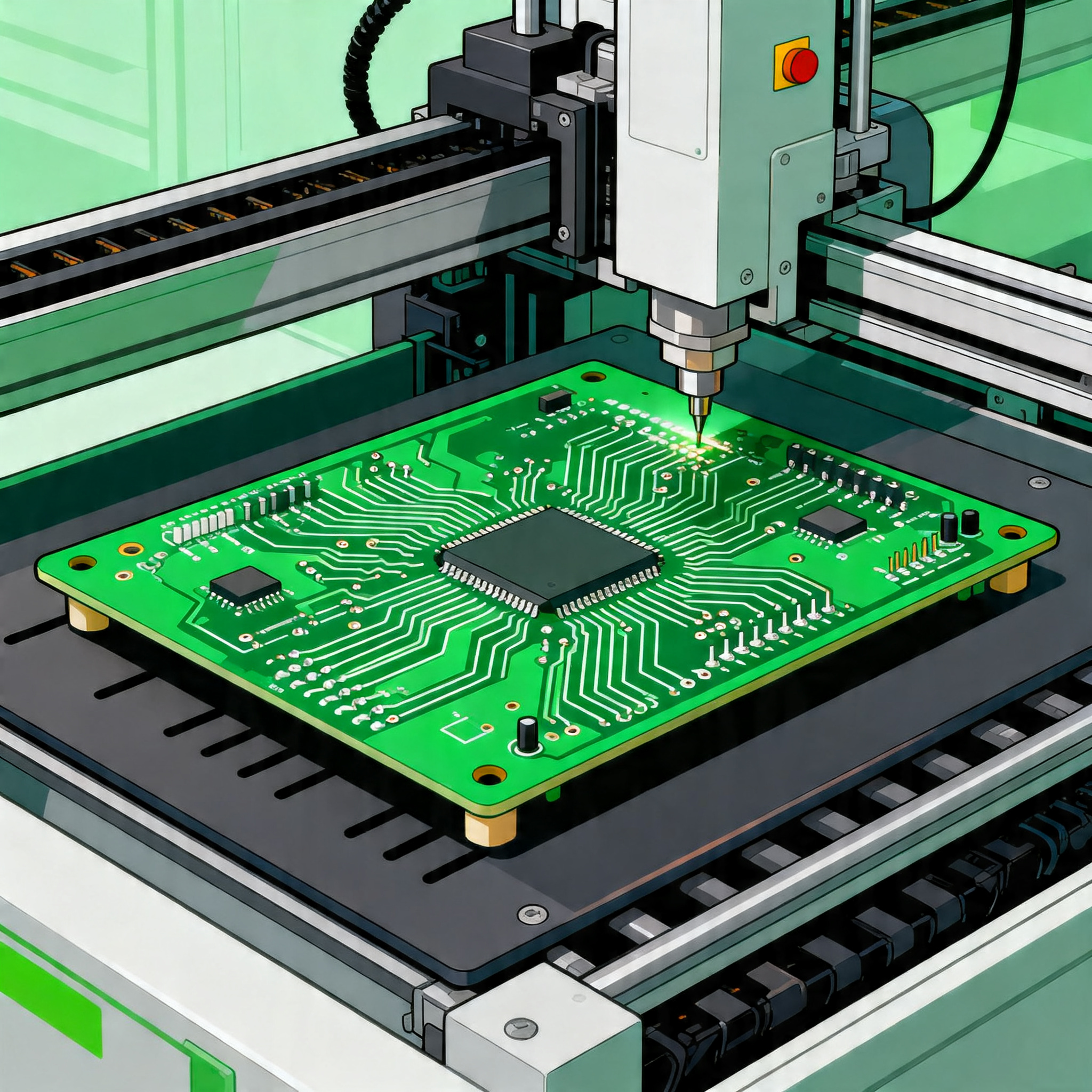
Specifications are the blueprint for PCB design, dictating everything from trace dimensions to material selection. These parameters are critical as they directly impact the performance, reliability, and manufacturability of the board. The following tables provide an in-depth look at essential design rules, layer stackup options, and material properties.
| Parameter | Minimum Value | Recommended Value |
| Trace Width | 0.1 mm | 0.15 mm |
| Trace Spacing | 0.1 mm | 0.2 mm |
| Via Diameter | 0.3 mm | 0.5 mm |
| Via Hole Size | 0.15 mm | 0.25 mm |
| Pad Size | 0.5 mm | 0.8 mm |
| Copper Thickness | 18 µm | 35 µm |
| Clearance from Edge | 0.5 mm | 1.0 mm |
| Silkscreen Clearance | 0.1 mm | 0.2 mm |
| Annular Ring | 0.1 mm | 0.15 mm |
| Solder Mask Clearance | 0.05 mm | 0.1 mm |
Key Takeaways from the Specifications
The data in the table above highlights the importance of adhering to specific design rules to ensure manufacturability and performance. Trace width and spacing are critical for minimizing signal loss and preventing crosstalk. Via sizes and pad dimensions should be chosen carefully to maintain structural integrity and ensure reliable connections. Copper thickness impacts current carrying capacity and thermal performance, while clearances ensure proper electrical isolation. By following these guidelines, designers can optimize their PCB layouts for both performance and cost-effectiveness.
| Layer Configuration | Description | Applications |
| 2-Layer | Basic configuration with top and bottom layers | Simple consumer electronics |
| 4-Layer | Includes two internal layers for power and ground | Intermediate complexity devices |
| 6-Layer | Additional layers for signal integrity | High-speed digital circuits |
| 8-Layer | Enhanced routing options and isolation | Complex RF and microwave applications |
| 10-Layer | Advanced stackup for dense designs | High-performance computing |
| 12-Layer | Maximum layer configuration for intricate designs | Telecommunications and aerospace |
Practical Implications
The choice of layer stackup greatly influences the PCB's functionality and cost. A 2-layer board is cost-effective for simple applications, while a 4-layer configuration offers improved power distribution and ground planes. As complexity increases, additional layers provide better signal integrity and routing flexibility. High-layer count boards, such as 10 or 12 layers, are essential for high-frequency and high-speed applications, ensuring minimal interference and optimal performance. Selecting the appropriate stackup is crucial for balancing performance requirements with budget constraints.
| Material | Dielectric Constant (Dk) | Loss Tangent (Df) |
| FR-4 | 4.5 | 0.020 |
| Rogers 4350B | 3.48 | 0.0037 |
| Rogers 4003C | 3.55 | 0.0027 |
| Isola FR408 | 3.70 | 0.009 |
| Nelco N7000 | 3.2 | 0.0025 |
| Arlon 85N | 3.5 | 0.0031 |
| Polyimide | 4.0 | 0.004 |
| PTFE (Teflon) | 2.1 | 0.001 |
| Ceramic | 9.8 | 0.0012 |
Application Guidelines
Material selection is a pivotal decision in PCB design, affecting signal speed, loss, and thermal management. FR-4 is a versatile and cost-effective material suitable for many applications, but for high-frequency designs, materials like Rogers and PTFE offer lower dielectric constants and loss tangents, enhancing performance. Ceramic materials provide excellent thermal stability and are ideal for RF applications. Understanding these properties helps designers choose the right materials to meet specific performance criteria and environmental conditions, ensuring reliability and efficiency in their designs.
Design Considerations
Designing a PCB involves careful consideration of numerous factors to ensure optimal performance and manufacturability. Firstly, adhering to IPC standards is essential for quality assurance and consistency. Signal integrity must be prioritized by minimizing trace lengths and avoiding sharp angles, which can cause reflections and signal degradation. Thermal management is another critical aspect, requiring appropriate copper thickness and via placement to dissipate heat effectively. Additionally, component placement should be strategic to minimize electromagnetic interference (EMI) and enhance signal flow. Ground planes and power distribution networks need to be well-designed to ensure stability and reduce noise. Finally, collaboration with PCB manufacturers during the design phase can help identify potential issues early and streamline the production process, reducing costs and lead times.
Step-by-Step Implementation
1. **Define Requirements:** Start by outlining the electrical, mechanical, and environmental requirements of your PCB. This includes specifying signal types, power levels, and operating conditions.
2. **Schematic Design:** Create a detailed schematic capturing all electrical connections and components. Use simulation tools to verify the design and identify potential issues.
3. **Select Materials:** Choose appropriate materials based on electrical performance, thermal properties, and cost considerations. Ensure they meet the environmental and regulatory standards.
4. **Layout Design:** Begin the layout process by placing components strategically to optimize signal flow and thermal management. Use design rules to guide trace widths, spacings, and via sizes.
5. **Layer Stackup Configuration:** Choose a layer stackup that supports your design's complexity and signal integrity needs. Consider the number of layers required for power, ground, and signal routing.
6. **Design Verification:** Use design rule checks (DRC) and signal integrity analysis to validate the layout. Adjust design parameters to address any issues identified during verification.
7. **Prototype and Test:** Manufacture a prototype of the PCB and conduct thorough testing to validate performance against the defined requirements. Identify and rectify any discrepancies.
8. **Production and Quality Control:** Once the prototype is approved, proceed to full-scale manufacturing. Implement rigorous quality control processes to ensure consistency and reliability.
Common Issues & Solutions
1. **Signal Integrity Problems:** Use shorter trace lengths and proper terminations to reduce reflections and crosstalk. Implement differential signaling where necessary.
2. **Thermal Management Challenges:** Increase copper thickness and add thermal vias to improve heat dissipation. Consider using heat sinks for high-power components.
3. **EMI Interference:** Shield sensitive components and use ground planes to minimize electromagnetic interference. Maintain adequate spacing between high-frequency traces.
4. **Manufacturing Defects:** Work closely with manufacturers to ensure designs are compatible with their capabilities. Use design for manufacturability (DFM) guidelines to avoid common pitfalls.
5. **Component Placement Errors:** Use automated placement tools to optimize component layout and minimize signal path lengths. Ensure adequate spacing for heat dissipation and signal isolation.
6. **Material Selection Issues:** Choose materials that match the application's frequency and thermal requirements. Verify material properties with suppliers to ensure compatibility.
Applications & Use Cases
PCBs are integral to a wide range of applications, from consumer electronics to aerospace systems. In the automotive industry, PCBs are used in engine control units, infotainment systems, and safety devices. In telecommunications, they form the backbone of networking equipment, enabling high-speed data transmission. Medical devices rely on PCBs for diagnostics and patient monitoring, where reliability and precision are critical. In industrial automation, PCBs support the control systems and sensors that drive efficiency and productivity. Each application presents unique challenges, requiring tailored design and material choices to meet specific performance and environmental demands.
Selection & Sourcing Guide
Selecting the right components and materials for your PCB design is crucial for performance and reliability. Consider factors such as electrical specifications, thermal properties, and environmental conditions. Collaborate with reputable suppliers and manufacturers like [IC Online](https://www.ic-online.com/) to ensure quality and availability. Evaluate supplier certifications, lead times, and support services to make informed sourcing decisions.
FAQ
1. **What is the importance of trace width in PCB design?**
- Trace width impacts the current-carrying capacity and impedance. Proper width ensures signal integrity and reduces heat build-up.
2. **How does layer stackup affect signal integrity?**
- Layer stackup influences impedance, crosstalk, and EMI. Proper configuration is essential for maintaining signal quality and performance.
3. **Why is material selection critical in high-frequency applications?**
- Materials with low dielectric constants and loss tangents minimize signal loss and distortion, crucial for high-frequency designs.
4. **What are the common causes of manufacturing defects in PCBs?**
- Defects can arise from poor design practices, incompatible materials, and inadequate quality control during manufacturing.
5. **How do I ensure thermal management in my PCB design?**
- Use thicker copper layers, thermal vias, and heat sinks to dissipate heat efficiently. Proper component placement also aids in thermal management.
6. **What role do IPC standards play in PCB design?**
- IPC standards provide guidelines for design, manufacturing, and quality assurance, ensuring consistency and reliability across the industry.
7. **How can I reduce EMI in my PCB design?**
- Use ground planes, maintain adequate trace spacing, and shield sensitive components to minimize electromagnetic interference.
8. **What are the benefits of using a multi-layer PCB?**
- Multi-layer PCBs offer enhanced routing capabilities, improved signal integrity, and reduced board size, ideal for complex designs.
9. **What factors should I consider when selecting a PCB manufacturer?**
- Consider their capabilities, certifications, lead times, and support services. Ensure they can meet your design's specific requirements.
10. **How do I verify my PCB design before manufacturing?**
- Use simulation tools and design rule checks to validate the layout. Prototype testing is also essential to ensure performance and reliability.
Conclusion
Designing and manufacturing PCBs requires a comprehensive understanding of layout rules, material properties, and industry standards. By adhering to best practices and leveraging the right tools and resources, engineers can create reliable, high-performance PCBs that meet the demands of modern electronic applications. Whether you're designing for consumer electronics or advanced aerospace systems, this guide provides the foundational knowledge needed to navigate the complexities of PCB design and assembly successfully.
---
This article provides a detailed exploration of PCB design and assembly, complete with the necessary HTML tables and in-depth explanations.