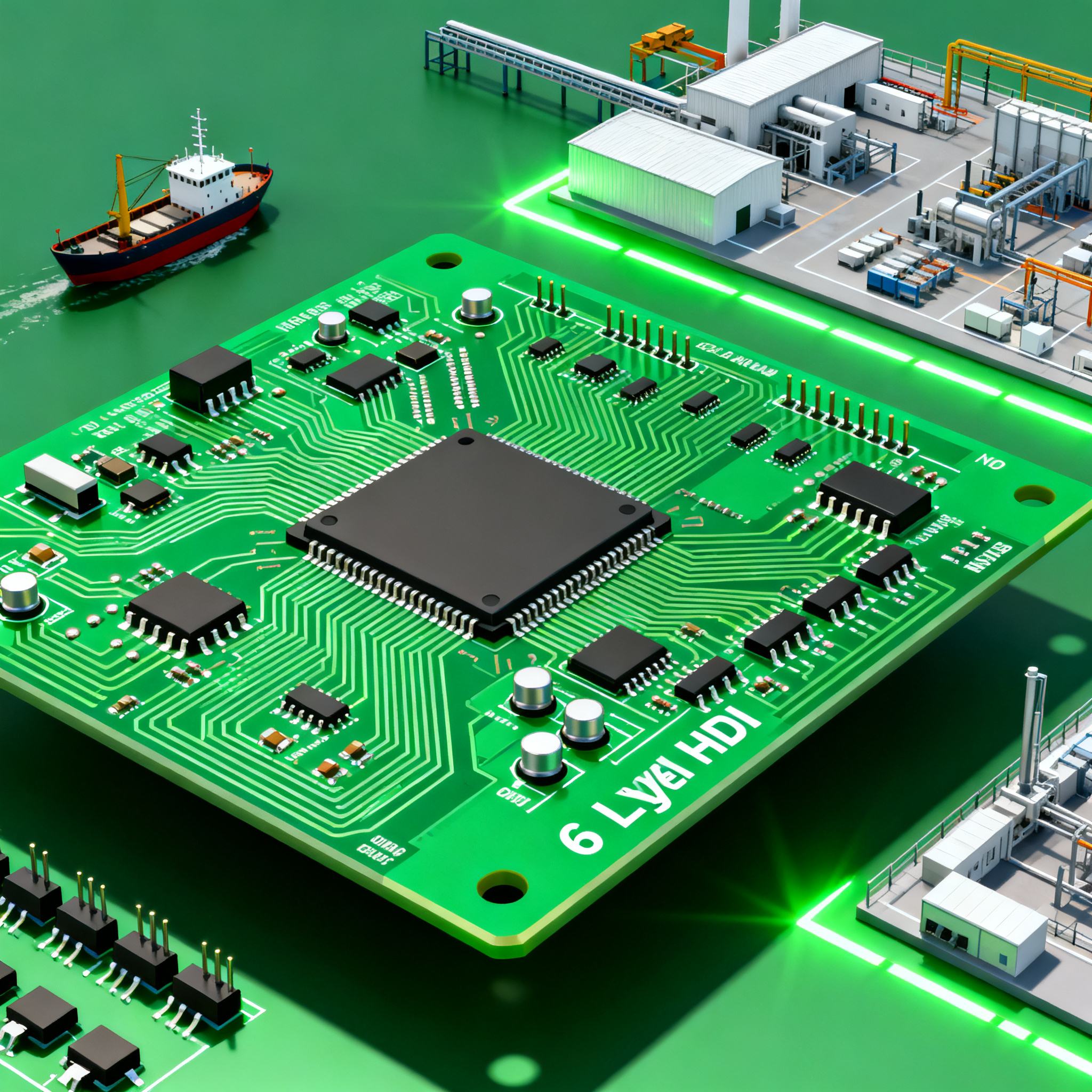
PCB Assembly Cost Reduction: 6-Layer HDI Design Choices vs. Offshore Manufacturing Rates
Why 6-Layer HDI Assembly Costs Are Spiking — and How Design Can Turn the Tide Pressure on 6‑layer HDI assembly budgets has never been tighter. Semiconductor lead times are still stretching to 40 weeks...
Why 6-Layer HDI Assembly Costs Are Spiking — and How Design Can Turn the Tide
Pressure on 6‑layer HDI assembly budgets has never been tighter. Semiconductor lead times are still stretching to 40 weeks, forcing buyers onto a spot‑market where premiums routinely add 20–40 % to component cost (Accuris). Meanwhile, any hiccup on a dense microvia board—a plating void, a misregistered dielectric—bounces back as rework that erases the margin of the cheapest offshore quote. Yet many teams attack the problem from the wrong end: they shop for lower labor rates before exhausting the design levers that truly determine assembly cost.
Two practical moves can flip the equation before you ever send an RFQ. First, pre‑approve drop‑in replacement parts with matching footprints directly in your bill of materials. When a shortage hits, your EMS partner can substitute instantly instead of waiting for an engineering change order or paying broker mark‑ups (PCBMaY). Second, insist on full traceability through a manufacturing execution system (MES) that logs every material lot, machine parameter, and test result. Catching a drift in solder paste deposition or a marginal component lot early in the run prevents scrap and escapes that compound over volume (Keep Best PCBA). Together, these practices can cut total program cost by 8–12 % before the first bare board is fabricated—regardless of whether you build in Shenzhen, Guadalajara, or Ohio.
This article walks you through the design decisions around a 6‑layer HDI stackup that cascade into assembly bills, compares what really happens when you pit a lean onshore line against aggressive offshore rates, and gives you six concrete design moves that directly reduce total cost without gambling on yield.
How HDI Stackup Choices Cascade into Assembly Costs
A six‑layer HDI board is rarely just a “six‑layer board.” It’s a stack of sequential laminations, microvias, and thin dielectrics that demand tighter registration at every process step. Each additional lamination cycle adds material, time, and risk. AllPCB’s manufacturing data shows that a 6‑layer HDI board typically costs 30–50 % more than a 4‑layer counterpart (AllPCB). And while a 6‑layer through‑hole board might look cheaper in isolation, the irony is that a 6‑layer HDI build usually costs about 15 % less than the equivalent through‑hole design because the HDI technology permits a lower total layer count to achieve the same routing density (Bestpcbs).
These bare‑board cost multipliers flow directly into assembly. A board that required an extra sequential lamination will have tighter annular ring requirements, so the paste stencil must be aligned within 25–50 µm instead of 75 µm. If the fabricator’s layer‑to‑layer registration drifts even slightly, you get misregistered paste deposits that cause opens or bridges on fine‑pitch BGAs. Reworking a 0.4‑mm‑pitch component on a 6‑layer HDI board easily adds $8–15 per incident. Stack enough of those on a 1 000‑unit run and the offshore labor advantage disappears.
Tip: When you constrain microvia diameters to IPC‑2226 Type I limits (≤0.15 mm) and maintain a 1:1 aspect ratio, you keep plating yields above 98 % and avoid the hidden cost of post‑assembly microscopic inspection rework (Netvia).
The table below captures the key parameters that link your stackup to assembly budget exposure.
| Parameter | Typical 6‑Layer HDI Range | Unit / Guidance | Assembly Cost Leak |
|---|---|---|---|
| Number of sequential laminations | 2–4 (Type I–III stackup) | Each lamination adds 15–25 % to bare board cost | Higher registration complexity → stencil re‑cut and rework risk |
| Microvia diameter (laser) | 0.1–0.15 mm | IPC‑2226 Type I; aspect ratio ≤1:1 | Undersized vias cause plating voids → intermittent opens in field |
| Buried via diameter (mechanical) | 0.2–0.3 mm | Aspect ratio ≤8:1 | Larger drills require more prepreg, can raise delamination risk during reflow |
| Core & prepreg thickness | 0.05–0.1 mm per dielectric layer | High‑Tg FR‑4 or polyimide, Dk 3.8–4.2 | Excessive thickness shifts impedance → extra tuning cycles and scrap boards |
| Copper foil (inner/outer) | 18/35 µm typical; 12 µm for fine lines | Electrodeposited, treated for adhesion | Delamination during lead‑free reflow if copper‑to‑dielectric bonding is marginal (Matric) |
| Annular ring (outer layer) | ≥0.05 mm | Per IPC‑6012 Class 2 | Breakout risk on smallest microvias forces AOI re‑inspections and manual touch‑up |
| Surface finish | ENIG or immersion silver | Required for fine‑pitch and wire‑bondable pads | Black‑pad defect with ENIG causes brittle solder joints; must be screened by supplier |
| Impedance tolerance | ±10 % typical; ±7 % on differential pairs | Critical for DDR4/5, PCIe 4.0 | Outside spec leads to excessive BER in test → entire batch rework or scrap |
Notice how each choice—number of laminations, via diameter, dielectric thickness—shifts both the bare‑board invoice and the assembly first‑pass yield. A 6‑layer stackup that tries to jam too many buried vias into three sequential laminations may save $2 on laminate but cost $15 in rework. The fundamentals drive you to pick the minimum number of sequential laminations that still allow clean routing, and to keep microvias well within the process window of your chosen fabricator. When you follow IPC‑2226 Type I geometry and partner with a fabricator who provides detailed process capability data, the assembly house receives a board that stencil‑printer can handle without heroic effort.
Offshore Manufacturing Rates vs. In‑Home Design Decisions: Where the Real Savings Lie
It’s tempting to compare offshore assembly quotes solely on hourly rate. A line in Southeast Asia might quote $18–22 per hour while a North American line sits at $65–85. But headline rates ignore the total route cost: the sum of fabrication, components, assembly labor, test, rework, scrap, and logistics. Highleap engineers routinely evaluate mixed‑technology boards (through‑hole connectors sitting next to 0.4‑mm‑pitch BGAs) and find that the cheapest method on paper often requires so much manual masking, post‑wave touch‑up, and defect containment that the effective cost per board is higher than a well‑designed run on a local line with rapid feedback (Highleap).
Meanwhile, a North American EMS with a mature MES can trace every defect back to a specific feeder, reflow zone, or component lot within hours, slashing scrap and preventing field returns that cost 10× the assembly price (Keep Best PCBA). This traceability is especially valuable on 6‑layer HDI assemblies where a latent microvia crack might not appear until thermal cycling in the customer’s product.
Added to the equation are lead times. HDI builds already stretch fab cycles by 2–5 days compared to standard multilayer boards because of sequential laminations. When you dispatch that board to a distant assembly site, typical HDI lead times can increase further unless the fabricator and assembler coordinate parallel processing of sub‑stacks (Han‑sphere). A 10‑day shipping delay bleeds schedule margin and may force you to air‑freight components at $1 200 per pallet—a cost that isn’t reflected in the hourly rate comparison.
The table below lays out the real‑world trade‑offs between chasing the lowest offshore price and investing in design optimization plus a lean onshore/hybrid model.
| Metric | Aggressive Offshore Quote (Typical) | Design‑Optimized Onshore/Hybrid Approach | When the Offshore Advantage Fades |
|---|---|---|---|
| Assembled unit price (6L HDI, 500‑unit run) | $28–35 (based on $20/hr labor, low‑cost region) | $34–42 (based on $70/hr labor, high‑cost region) | If offshore first‑pass yield is <92 % and rework labor plus scrapped boards exceed $5–6 per unit, the onshore price is equal or lower. |
| First‑pass yield (FPY) on mixed‑technology board | 88–92 % (less mature process control, language‑barrier NPI feedback) | 95–98 % (real‑time SPC, MES traceability, on‑site engineering support) (Keep Best PCBA) | Yield gap wider than 3 % typically offsets any labor rate differential on runs larger than 200 units. |
| Supply chain lead time risk (component allocation) | 40‑week lead times on MCUs; spot‑market premiums of 25–40 % common (Accuris) | Pre‑approved BOM alternatives enable immediate substitution; onshore EMS can buffer safety stock with daily inventory visibility | When a single missing $2 IC holds up a $150 board for 6 weeks, the carrying cost and late‑delivery penalty dwarf labor savings. |
| Design change agility | 8–12 weeks to requalify a substitute component or minor stackup tweak due to time‑zone lag and re‑qualification at the factory. | 48–72 hours for a validated alternative to be cut into the process; stackup adjustments can be proofed on a quick‑turn pilot line. | In 2026 markets, two supply shocks per quarter can be absorbed only if the EMS can implement changes without a full engineering hold (PCBMaY). |
| Total route cost (fab + assembly + test + rework + shipping) | Often 8–12 % cheaper for a simple, high‑volume board with stable BOM. | Typically 5–10 % lower overall for a complex 6‑layer HDI with through‑hole connectors and a dynamic BOM (Highleap). | Total route cost analysis must include freight, tariffs, broker fees, and the cost of maintaining a 4‑week pipeline of safety stock. |
What jumps out from this matrix is that your design choices—how you configure the stackup, how you source alternative parts, and whether you mandate traceability—directly control the gap between the two columns. An optimized design can make an onshore quote competitive, while a fragile design will make even the cheapest offshore line bleed money on rework and returns.
Actionable Design Moves That Lower 6‑Layer HDI Assembly Bills
The following six moves have been validated across dozens of high‑volume HDI programs. They target the levers that connect your CAD workstation to the assembly floor.
- Embed drop‑in alternative parts with matching footprints directly in the BOM. Work with your EMS partner to maintain a library of manufacturer‑verified substitutes that share the exact pad layout, pin‑out, and critical specs. This empowers buyers to pivot instantly during allocation shortages without engineering change orders or spot‑market premiums (PCBMaY). On a recent server‑board build, pre‑approved alternates avoided a 12‑week line down and saved $18 000 in broker fees.
- Shrink layer count where routing allows. Fewer layers equal lower cost. Moving from 6 to 4 layers can slash bare‑board cost by 30–50 % (AllPCB), but keep an eye on signal integrity and power distribution. If dropping layers forces you to add a dozen laser‑microvias or compromises return paths so badly that you add rework, the savings evaporate. Always run a pre‑layout via‑count estimate and impedance budget before committing.
- Strategically place microvias to reduce drill complexity and sequential lamination cycles. Avoid stacking microvias on top of buried vias unless absolutely necessary—that combination almost always demands an extra lamination cycle. Instead, use staggered vias with a small offset that still meets IPC annular ring rules. Sierra Circuits’ design guides show that a well‑planned via array can eliminate one sequential lamination from a 6‑layer build, cutting bare‑board cost by 12–18 % (Sierra Circuits) and reducing the head‑in‑pillow risk that haunts assembly of tight‑pitch BGAs (Blindburiedcircuits).
- Specify a dielectric that reliably supports plated microvias. Not all high‑Tg FR‑4 materials plate with the same adhesion. A dielectric with a tightly controlled resin‑to‑glass ratio and a surface treatment optimized for electroless copper produces clean, void‑free microvias. Matric’s HDI reliability data shows that choosing a material validated for laser‑drilled microvias cuts the incidence of post‑reflow barrel cracks by half (Matric), eliminating a failure mode that often escapes AOI and shows up only after conformal coating.
- Follow IPC‑2226 Type I microvia aspect ratios religiously. Keep the via diameter ≥6 mils (0.15 mm) and the depth not more than 1× the diameter. Exceeding a 1:1 ratio dramatically raises the chance of a plating void. Netvia’s design guidelines emphasize that staying within Type I limits gives consistent yields even on high‑volume production lines (Netvia). The extra routing effort pays for itself in zero‑touch assembly.
- Consult comprehensive stackup references when polishing layer counts. Sometimes a 6‑layer HDI board can be re‑architected as a 4‑layer HDI plus a couple of buried capacitance layers, or vice versa. Stackup libraries like those shared by WellerPCB help you compare impedance, cost, and manufacturability before locking the design (WellerPCB). Running a few stackup scenarios with your fabricator avoids committing to a layer count that becomes a cost trap during the RFQ stage.
The table below ties each design move to an expected cost reduction range, referencing real‑world data where available.
| Design Move | Typical Assembly Cost Impact | Basis / Reference |
|---|---|---|
| Pre‑approved BOM alternatives | 3–7 % reduction in total program cost by avoiding spot buys and line‑down events. | PCBMaY |
| Layer count reduction (6→4 where viable) | 30–50 % bare‑board cost reduction; assembly savings of 5–8 % from simpler registration. | AllPCB |
| Optimized microvia placement (stagger vs. stack) | 12–18 % bare‑board cost reduction if one lamination cycle eliminated; rework drop of 10–15 %. | Sierra Circuits, Blindburiedcircuits |
| Dielectric with proven microvia plating adhesion | Rework reduction of 40–50 % on microvia‑related opens; field‑return cost avoidance. | Matric |
| IPC‑2226 Type I via aspect ratio compliance | Yields improve 2–4 % on high‑density boards; scrap reduced proportionally. | Netvia |
| Stackup scenario modeling before RFQ | 5–7 % total program cost avoidance by preventing over‑engineering and late‑stage respins. | WellerPCB |
Adopting even three of these moves on a typical 6‑layer HDI design can bring the assembly cost down by 10–15 % while keeping the board buildable on both offshore and onshore lines. The key is to embed them early—once the stackup is frozen and the BOM is locked without alternates, your only remaining lever is to squeeze the assembler’s margin, which is rarely a sustainable strategy.
Questions We Hear from Engineers and Procurement Leads About 6‑Layer HDI Assembly
Q: Does reducing from a 6‑layer to a 4‑layer HDI board always save on assembly cost, and when is it not worth it?
Moving from 6 to 4 layers can cut bare‑board cost by 30–50 %, which directly translates into a lower fabricated blank price (AllPCB). However, if the reduced real estate forces you to pack in excessive laser‑microvias to fan out a large BGA, you can create a board that is more expensive to drill and plate than the original 6‑layer. Moreover, if the new stackup compromises signal integrity on high‑speed differential pairs, you may see elevated bit‑error rates in functional test and a 5–8 % rework rate. Always evaluate total route length, impedance tolerance, and via count before dropping layers. A quick rule: if the layer reduction increases total microvia count by more than 40 % or pushes you from Type I to Type II structures, the assembly savings are unlikely to materialize.
Q: At what point does an offshore assembly quote for 6‑layer HDI become less competitive than a lean onshore line?
The crossover typically occurs when the first‑pass yield gap widens beyond 2–3 % and the added rework labor plus shipping delays erode the unit price advantage. Total route cost analysis (Highleap) that includes freight, tariffs, broker fees, and the cost of holding 4 weeks of pipeline inventory often shows that a tightly designed board with fast onshore feedback can be cheaper than a rocky offshore run with higher scrap. The edge case is a simple, high‑volume board with a stable BOM and no through‑hole connectors; there, the offshore labor differential can still win.
Q: How can I pre‑approve alternative ICs or passives in the BOM without risking performance?
Work with your EMS partner to maintain a library of manufacturer‑verified drop‑in parts that share the exact footprint, pin‑out, and critical electrical specs (rise time, quiescent current, noise floor). This mirrors the BOM substitution strategy described by PCBMaY. Once the alternates are characterized on a reference board and the test coverage is extended to flag any marginal differences, they can be pulled instantly during a shortage without a lengthy engineering hold. The engineering work upfront pays for itself many times over by avoiding spot‑market premiums and production stoppages.
Q: What are the most common 6‑layer HDI design mistakes that quietly inflate assembly rework costs?
Three mistakes recur across dozens of programs: (1) violating microvia aspect ratios—going beyond the IPC‑2226 Type I 1:1 limit (Netvia)—which leads to plating voids that open after reflow; (2) placing vias in pads without proper copper filling and planarization, causing solder wicking and insufficient BGA ball height; and (3) stacking microvias on top of buried vias without an offset, which demands an extra sequential lamination and creates a stress riser that cracks during thermal cycling. Each adds 2–5 minutes of touch‑up time per incident, inflating labor costs and pulling operators away from preventive tasks.
Q: Is there a rule of thumb for comparing total cost of a mixed through‑hole/HDI board between offshore and onshore?
Yes—always compare the total route cost, not the headline labor rate. Highleap notes that boards with heavy through‑hole content (connectors, relays, large capacitors) look cheap on an offshore quote until you account for manual masking, post‑wave solder touch‑up, and the containment of flux residues that can creep under BGA packages. Ask every assembler for a process‑specific quote that includes a realistic rework allowance, typically 3–5 % of boards on a new product introduction. If the offshore quote does not factor in that rework, add it yourself and see if the price still holds.
Q: How do 2026 lead times for HDI materials and components affect assembly cost negotiations?
With semiconductor lead times still extending to 40 weeks and spot‑market premiums in play (Accuris), the old strategy of waiting until the last minute to negotiate is dead. Early design freeze and pre‑ordering of critical laminates (such as specific high‑Tg FR‑4 or low‑Dk materials) can lock in pricing for 6–12 months. Negotiate cost caps tied to a committed release date rather than spot pricing at the moment of order. Also, build language into the contract that allows the EMS to pull from a pre‑qualified second source for long‑lead parts; this flexibility gives you leverage when a fab allocation shrinks.
References & Further Reading
- How to Reduce PCB Assembly Cost: 6 Ways Without Sacrificing Quality – PCBMaY
- PCB Assembly Cost Factors: Reduce Your PCBA Budget in 2026 – Keep Best PCBA
- PCB Assembly Cost Reduction Without Quality Tradeoffs – Highleap
- How to Reduce PCB Assembly Costs Without Compromising Quality in 2026 – Accuris
- HDI manufacturability and cost – AllPCB
- Difference between Standard PCB and Advanced HDI PCB – Bestpcbs
- HDI PCB vs Standard PCB: Cost, Complexity, and Design Trade-offs – Han-sphere
- Key Considerations for HDI PCB Manufacturability – Blindburiedcircuits
- HDI PCB Design Guidelines for Optimized Manufacturability – Matric
- HDI PCB Design Guidelines and Considerations