Optimizing PCB Design for Electrical Performance: Key Considerations for Engineers
Optimizing PCB Design for Electrical Performance: Key Considerations for Engineers table { border-collapse: collapse; width: 100%; margin: 20px 0; } th, td { border: 1px solid #ddd; padding: 8px; } th...
Introduction
In the rapidly evolving field of electronics, optimizing Printed Circuit Board (PCB) design for electrical performance is crucial. Engineers face challenges such as increasing complexity, miniaturization, and the need for higher efficiency. Effective PCB design not only ensures device reliability but also enhances performance and reduces manufacturing costs. Understanding key considerations, such as component specifications, datasheets, and application circuits, is essential for achieving optimal electrical performance in your designs.
Technical Overview
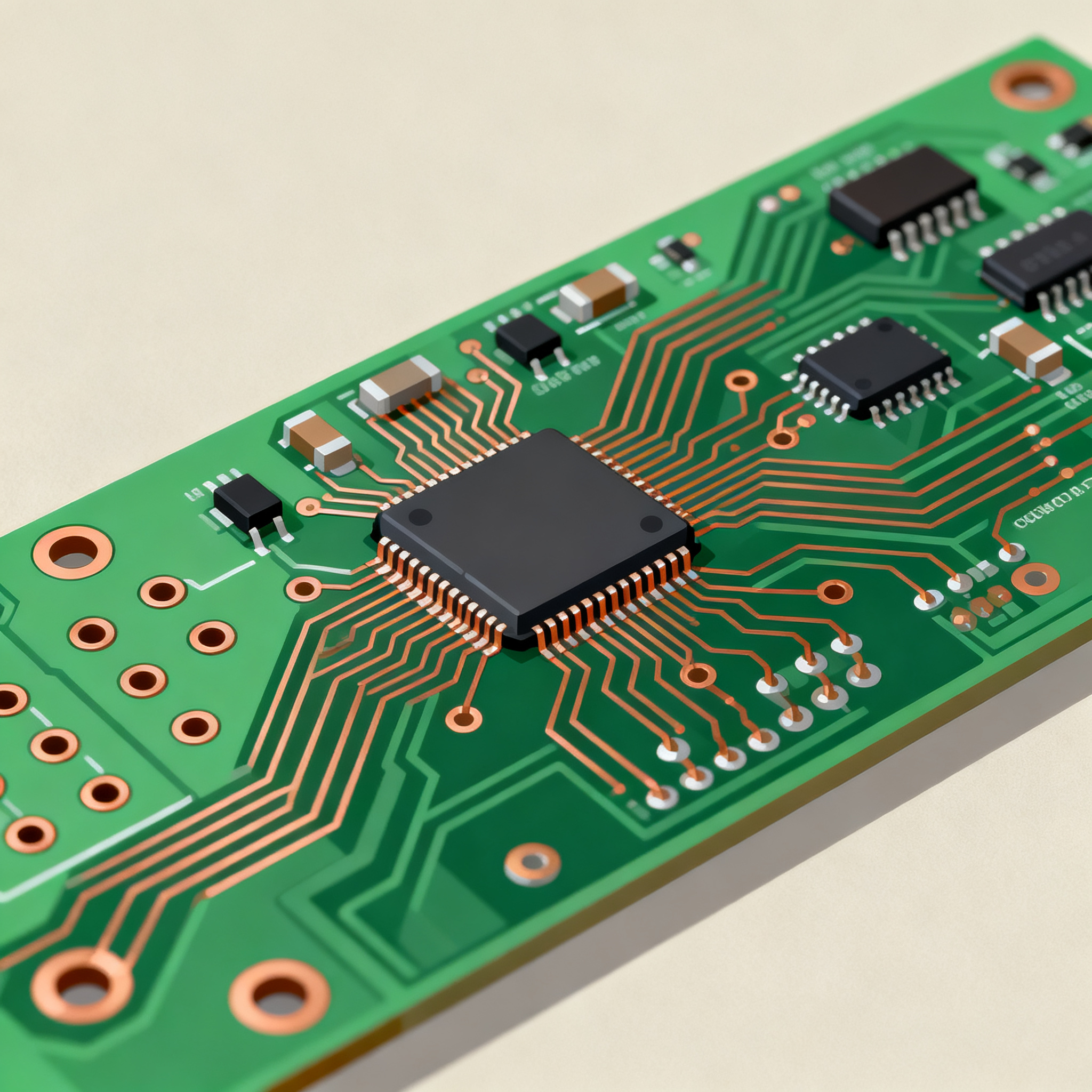
PCB design involves a complex interplay of various components and principles. At its core, a PCB serves as the backbone for electronic components, providing the necessary electrical pathways for signal transmission. The architecture of a PCB must accommodate various elements, including integrated circuits (ICs), resistors, capacitors, and connectors. Factors such as trace width, layer count, and signal integrity play a critical role in the board's performance. Engineers must also consider thermal management, electromagnetic compatibility (EMC), and manufacturability. By understanding these core concepts, engineers can design PCBs that meet stringent electrical performance criteria while adhering to industry standards, such as those outlined by the IPC.
Detailed Specifications
When designing a PCB, understanding the specifications of each component is crucial. These specifications, often found in datasheets, provide essential information on the component's capabilities and limitations. Key specifications include CPU speed, memory, peripherals, power requirements, and the physical package of the component. Understanding these parameters helps engineers select the right components for their applications and ensures compatibility with other elements of the design.
| Specification | Description | Typical Values |
|---|---|---|
| CPU Speed | Processor speed of the IC | 1.2 GHz - 3.5 GHz |
| Memory | On-chip memory capacity | 512 KB - 8 MB |
| Peripherals | Available interfaces and controllers | I2C, SPI, UART, USB |
| Power Supply | Operating voltage range | 1.8V - 5.5V |
| Package Type | Physical form factor | LQFP, BGA, QFN |
| Temperature Range | Operational temperature limits | -40°C to 85°C |
| Clock Frequency | Maximum clock speed | 20 MHz - 200 MHz |
| GPIO Pins | General-purpose I/O pins | 16 - 128 pins |
| ADC Resolution | Analog-to-digital converter resolution | 8-bit - 12-bit |
| DAC Channels | Digital-to-analog converter channels | 1 - 4 channels |
Key Takeaways from the Specifications
The data in Table 1 highlights the critical specifications engineers must consider when selecting components for PCB design. CPU speed and memory capacity determine the processing power and data handling capabilities of a system. Peripherals like I2C and SPI provide essential connectivity options, while power supply specifications ensure the component can operate within the desired voltage range. Package type influences the physical layout and soldering process. Understanding these specifications allows engineers to make informed decisions, ensuring that each component integrates seamlessly into their design, meeting both performance and environmental requirements.
| Characteristic | Description | Typical Values |
|---|---|---|
| Supply Voltage | Voltage required for operation | 3.3V - 5V |
| Operating Current | Current consumption during operation | 10 mA - 500 mA |
| Standby Current | Current consumption in standby mode | 0.1 mA - 10 mA |
| Input Voltage Range | Acceptable voltage range for inputs | 0V - 3.6V |
| Output Voltage | Voltage level at outputs | 0V - 3.3V |
| Propagation Delay | Time taken for signal to propagate | 5 ns - 50 ns |
| Max Clock Frequency | Maximum frequency of operation | 50 MHz - 150 MHz |
| ESD Protection | Electrostatic discharge protection level | 2 kV - 8 kV |
| Noise Margin | Acceptable noise range for signals | 0.4V - 1V |
| Output Impedance | Impedance of output drivers | 10 ohms - 50 ohms |
| Input Capacitance | Capacitance at input pins | 5 pF - 20 pF |
Practical Implications
The electrical characteristics outlined in Table 2 are vital for ensuring that components perform reliably under different operating conditions. Understanding supply voltage and current requirements helps in power management and thermal design. Propagation delay affects the timing and synchronization of signals, which is crucial for high-speed applications. ESD protection and noise margin are critical for ensuring signal integrity and reliability in harsh environments. By analyzing these characteristics, engineers can design circuits that are robust, efficient, and meet specific application needs, thereby enhancing the overall performance of the PCB.
| Use Case | Configuration | Considerations |
|---|---|---|
| Consumer Electronics | Low power, compact size | Battery life, cost efficiency |
| Industrial Automation | High reliability, robust | Temperature range, EMI resistance |
| Automotive Systems | High performance, safety | Thermal management, fault tolerance |
| Medical Devices | Precision, low noise | Regulatory compliance, reliability |
| Telecommunications | High speed, data integrity | Signal integrity, low latency |
| IoT Devices | Low power, connectivity | Battery efficiency, wireless protocols |
| Wearable Technology | Ultra-low power, small form factor | Comfort, battery life |
| Aerospace Applications | Extreme reliability, lightweight | Radiation resistance, vibration tolerance |
Application Guidelines
Table 3 provides a comparison of different applications and their specific configurations. Each use case demands unique considerations, such as power efficiency in consumer electronics and reliability in industrial automation. Automotive systems require stringent safety and thermal management, while medical devices focus on precision and regulatory compliance. By understanding these application-specific requirements, engineers can tailor their PCB designs to meet the challenges of each industry, ensuring that the final product not only performs optimally but also adheres to relevant standards and regulations.
Design Considerations
When designing a PCB, engineers must consider several key factors to optimize electrical performance. These include trace width and spacing, which affect the board's impedance and signal integrity. Proper layer stacking and component placement are critical for minimizing electromagnetic interference (EMI) and ensuring thermal management. Via design and ground plane considerations also play a significant role in signal routing and power distribution. Additionally, selecting the right materials and finishes can impact the board's durability and reliability. By adhering to design guidelines and IPC standards, engineers can create PCBs that are not only efficient but also manufacturable and cost-effective.
Step-by-Step Implementation
Implementing an optimized PCB design involves a systematic approach. Here are the key steps:
- Define Requirements: Understand the application's electrical and mechanical requirements, including power, size, and environmental constraints.
- Select Components: Choose components based on specifications and datasheets, considering factors like power consumption, package type, and cost.
- Design Schematic: Create a detailed schematic that outlines the electrical connections and component placements.
- PCB Layout: Use CAD software to design the PCB layout, focusing on trace routing, layer stacking, and component placement for optimal performance.
- Simulate and Analyze: Perform simulations to analyze signal integrity, thermal performance, and EMI compliance.
- Prototype and Test: Manufacture a prototype and conduct rigorous testing to validate the design against specifications.
- Iterate and Optimize: Make necessary adjustments based on test results to address any issues or improve performance.
- Finalize and Document: Once optimized, finalize the design and create comprehensive documentation for manufacturing and assembly.
Common Issues & Solutions
PCB design often encounters several common issues. Here are some typical problems and their solutions:
- Signal Integrity Issues: Use proper trace impedance and routing techniques to minimize reflections and crosstalk.
- Thermal Management: Implement heat sinks, thermal vias, and appropriate materials to dissipate heat effectively.
- EMI/EMC Compliance: Employ shielding, filtering, and proper grounding techniques to reduce electromagnetic interference.
- Power Distribution Problems: Ensure adequate power plane design and decoupling capacitors to maintain stable voltage levels.
- Manufacturing Defects: Follow DFM guidelines and perform thorough quality inspections to minimize defects during production.
- Component Placement Errors: Use automated tools and design rules to ensure accurate and efficient component placement.
Applications & Use Cases
Optimized PCB designs find applications across various industries. In consumer electronics, they enhance device performance while maintaining cost efficiency. In industrial automation, reliable PCBs ensure seamless operation under harsh conditions. Automotive systems benefit from high-performance PCBs that meet safety standards. Medical devices rely on precise and low-noise designs for accurate diagnostics. Telecommunications demand high-speed data integrity, while IoT devices require low power consumption and connectivity. By tailoring PCB designs to these specific use cases, engineers can create products that meet the unique demands of each industry.
Selection & Sourcing Guide
Selecting the right components and sourcing them efficiently is crucial for successful PCB design. Engineers can utilize online resources like IC Online to access a wide range of components and compare specifications. It's essential to consider factors such as lead time, cost, and supplier reliability when sourcing components. By leveraging these resources, engineers can ensure that they have the right components on hand to meet project timelines and performance requirements.
FAQ
- What is the importance of trace width in PCB design? Trace width affects the impedance and current-carrying capacity of the circuit, impacting signal integrity and thermal management.
- How can I minimize EMI in my PCB design? Use proper shielding, filtering, and grounding techniques, and follow EMI/EMC compliance guidelines.
- What is the role of a ground plane in a PCB? A ground plane provides a reference point for signals, reduces noise, and improves signal integrity.
- How do I choose the right PCB material? Consider factors like dielectric constant, thermal conductivity, and cost based on the application's requirements.
- What are the benefits of using a multilayer PCB? Multilayer PCBs allow for more complex designs, improved signal integrity, and better thermal management.
- How can I ensure my PCB design is manufacturable? Follow Design for Manufacturability (DFM) guidelines and collaborate with your manufacturing partner early in the design process.
- What is the significance of ESD protection in PCB design? ESD protection prevents damage to components from electrostatic discharge, ensuring reliability and longevity.
- How do I select the right package type for my components? Consider factors like space constraints, thermal performance, and assembly process when choosing a package type.
- Why is thermal management important in PCB design? Thermal management ensures that components operate within safe temperature limits, preventing overheating and failure.
- What tools can I use for PCB simulation and analysis? Use software tools like SPICE, Altium Designer, or Cadence Allegro for simulation and analysis of your PCB design.
Conclusion
Optimizing PCB design for electrical performance is a multifaceted challenge that requires careful consideration of component specifications, electrical characteristics, and application requirements. By understanding these key considerations and leveraging available resources, engineers can design PCBs that meet the demands of modern electronics while ensuring reliability, efficiency, and cost-effectiveness. Through meticulous planning, simulation, and testing, engineers can achieve optimal performance and drive innovation in their respective fields.