Navigating the PCB Manufacturing Process Flow: Key Stages for 4-Layer Boards
Navigating the PCB Manufacturing Process Flow: Key Stages for 4-Layer Boards Introduction In the rapidly evolving field of electronics, Printed Circuit Boards (PCBs) play a pivotal role as the backbon...
Introduction
In the rapidly evolving field of electronics, Printed Circuit Boards (PCBs) play a pivotal role as the backbone of nearly all electronic devices. The complexity of PCB design and manufacturing has increased significantly, especially with the advent of multi-layer boards such as 4-layer PCBs. Understanding the intricacies of the PCB manufacturing process is crucial for engineers and manufacturers alike, as it ensures the production of reliable and high-performance boards. This article delves into the key stages of the PCB manufacturing process flow, focusing on layout rules, stackup design, signal integrity, and manufacturing considerations.
Technical Overview
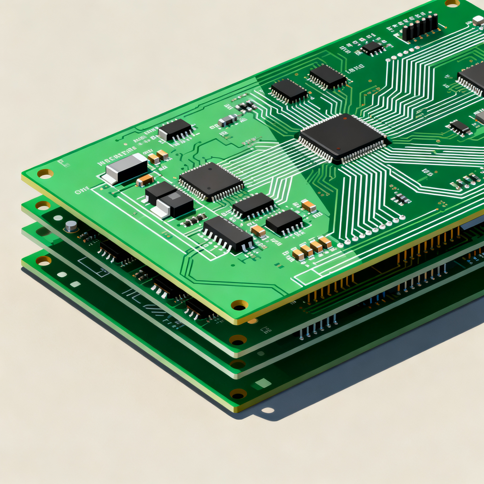
The manufacturing of a 4-layer PCB involves several critical stages that ensure the board functions as intended in its final application. The architecture of a 4-layer board typically includes two signal layers and two internal layers for power and ground planes, which help in reducing electromagnetic interference (EMI) and improving signal integrity. Core concepts such as trace width, spacing, and via sizes are fundamental to the PCB design rules, while stackup design determines the arrangement of layers and materials used. Signal integrity is maintained by controlling the impedance and minimizing noise, which is critical for high-frequency applications. Manufacturing considerations include the selection of appropriate materials, adherence to industry standards like IPC, and ensuring the board meets quality inspection criteria.
Detailed Specifications
When designing a 4-layer PCB, several specifications must be considered to ensure optimal performance and manufacturability. These specifications encompass PCB design rules, layer stackup options, and material properties. Each of these elements plays a vital role in the board's functionality and reliability. Understanding these specifications helps in making informed decisions during the design and manufacturing process.
| Design Rule | Minimum Value | Typical Value |
|---|---|---|
| Trace Width | 0.2 mm | 0.3 mm |
| Trace Spacing | 0.2 mm | 0.3 mm |
| Via Diameter | 0.6 mm | 0.8 mm |
| Via Hole Size | 0.3 mm | 0.4 mm |
| Pad Diameter | 0.5 mm | 0.7 mm |
| Clearance to Edge | 0.5 mm | 1.0 mm |
| Annular Ring | 0.1 mm | 0.15 mm |
| Power Plane Clearance | 0.2 mm | 0.3 mm |
| Silkscreen Clearance | 0.1 mm | 0.2 mm |
| Minimum Hole Size | 0.2 mm | 0.3 mm |
| Aspect Ratio | 8:1 | 10:1 |
Key Takeaways from the Specifications
Understanding the PCB design rules is critical for ensuring the manufacturability and reliability of 4-layer boards. The trace width and spacing influence the current-carrying capacity and signal integrity of the board. Adhering to the minimum values is essential for high-density designs, while typical values provide a buffer for manufacturing tolerances. Via sizes and pad diameters affect the mechanical strength and electrical connectivity of components. These specifications must align with the capabilities of your chosen PCB manufacturer to avoid costly redesigns and production delays.
| Stackup Configuration | Layer Description | Application |
|---|---|---|
| 1-2-3-4 | Signal-Power-Ground-Signal | Standard digital circuits |
| 1-2-3-4 | Signal-Ground-Power-Signal | High-speed applications |
| 1-2-3-4 | Power-Signal-Signal-Ground | RF applications |
| 1-2-3-4 | Ground-Signal-Power-Signal | Low EMI designs |
| 1-2-3-4 | Signal-Signal-Power-Ground | Analog circuits |
| 1-2-3-4 | Signal-Power-Signal-Ground | Mixed-signal designs |
| 1-2-3-4 | Ground-Power-Signal-Signal | Power distribution |
Practical Implications
The choice of layer stackup plays a significant role in the performance and efficiency of a 4-layer PCB. Different configurations cater to specific applications, such as high-speed digital circuits or RF applications. For example, placing ground and power planes adjacent can minimize EMI and enhance signal integrity. Selecting the appropriate stackup configuration ensures optimal thermal management and electrical performance, which is crucial for maintaining the reliability of high-frequency or power-intensive designs.
| Material | Dielectric Constant | Loss Tangent |
|---|---|---|
| FR-4 | 4.5 | 0.02 |
| Rogers 4350B | 3.66 | 0.0037 |
| Rogers 4003C | 3.55 | 0.0027 |
| Isola FR408 | 3.75 | 0.009 |
| Nelco N4000-13 | 3.7 | 0.008 |
| Arlon 85N | 3.5 | 0.008 |
| Megtron 6 | 3.5 | 0.004 |
| Polyimide | 3.5 | 0.004 |
| Teflon | 2.1 | 0.0002 |
Application Guidelines
The selection of materials for a 4-layer PCB greatly influences its electrical properties and thermal performance. FR-4 is a common choice due to its cost-effectiveness and adequate performance for most applications, but for high-frequency or precision circuits, materials like Rogers or Megtron offer superior dielectric properties and lower loss tangents. Selecting materials with appropriate dielectric constants and loss tangents is essential for maintaining signal integrity and minimizing power losses, especially in RF and high-speed digital applications.
Design Considerations
Designing a 4-layer PCB requires careful consideration of various factors to ensure optimal performance and manufacturability. Key considerations include:
- Signal Integrity: Proper trace routing, impedance matching, and minimizing crosstalk are essential for maintaining signal quality.
- Thermal Management: Adequate heat dissipation through thermal vias, heat sinks, and copper pours helps prevent overheating.
- Power Distribution: Efficient power plane design and decoupling capacitors ensure stable power delivery to all components.
- Manufacturability: Compliance with IPC standards and design for manufacturability (DFM) guidelines reduces production costs and time.
- Component Placement: Strategic placement of components minimizes signal path lengths and improves assembly efficiency.
Step-by-Step Implementation
Implementing a 4-layer PCB design involves several steps, each crucial for ensuring the final product meets the desired specifications and functions reliably:
- Define Requirements: Outline the electrical, mechanical, and environmental requirements for the PCB.
- Choose Materials: Select the appropriate substrate and dielectric materials based on performance and cost considerations.
- Design Schematic: Develop a detailed circuit schematic, ensuring all components and connections are accurately represented.
- Perform Layout: Use PCB design software to arrange components and route traces, adhering to design rules and layer stackup configurations.
- Simulate and Analyze: Conduct signal integrity and thermal simulations to identify potential issues and optimize the design.
- Generate Gerber Files: Create industry-standard Gerber files for manufacturing, ensuring all layers and drill files are included.
- Prototype and Test: Produce a prototype board, conduct thorough testing, and make any necessary design adjustments.
- Finalize Design: Incorporate feedback from testing, finalize the design, and prepare for full-scale manufacturing.
Common Issues & Solutions
Despite careful planning, several common issues can arise during the design and manufacturing of 4-layer PCBs. Here are some typical problems and their solutions:
- Signal Integrity Issues: Use controlled impedance traces and proper termination techniques to reduce signal degradation.
- Thermal Management Problems: Employ thermal vias and copper pours to enhance heat dissipation and prevent hotspots.
- Manufacturing Defects: Conduct thorough DFM checks and work closely with manufacturers to ensure adherence to design specifications.
- Component Misalignment: Utilize fiducial markers and precise alignment techniques to ensure accurate component placement.
- Power Distribution Challenges: Optimize power plane layouts and use adequate decoupling capacitors to maintain stable voltage levels.
- EMI Interference: Implement shielding techniques and proper grounding to minimize electromagnetic interference.
Applications & Use Cases
4-layer PCBs are widely used in various applications due to their ability to support complex circuitry and improve signal integrity. Common use cases include:
- Consumer Electronics: Smartphones, tablets, and laptops utilize 4-layer PCBs for compact and efficient circuit designs.
- Automotive Electronics: Advanced driver-assistance systems (ADAS) and infotainment systems benefit from the enhanced performance of multi-layer boards.
- Telecommunications: Networking equipment and communication devices often employ 4-layer PCBs for high-speed data transmission.
- Medical Devices: Precision medical instruments and diagnostic equipment rely on the reliability and compactness of 4-layer boards.
Selection & Sourcing Guide
When selecting and sourcing PCBs, it is essential to partner with reputable manufacturers that offer quality assurance and adhere to industry standards. Resources like IC Online provide access to a wide range of components and suppliers, making it easier to find the right PCB solutions for your needs. Consider factors like lead time, cost, and customization options when choosing a supplier.
FAQ
Here are some frequently asked questions related to 4-layer PCBs:
- What is the advantage of a 4-layer PCB over a 2-layer PCB? A 4-layer PCB offers improved signal integrity, reduced EMI, and better power distribution.
- How do I choose the right stackup for my application? Consider the signal frequency, EMI requirements, and thermal management needs when selecting a stackup configuration.
- What are the common materials used for 4-layer PCBs? FR-4, Rogers, and Teflon are commonly used materials, each offering different dielectric properties.
- How can I ensure my PCB design complies with IPC standards? Follow IPC design guidelines, conduct thorough DFM checks, and collaborate with experienced manufacturers.
- What simulation tools are recommended for PCB design? Tools like Altium Designer, Cadence Allegro, and Mentor Graphics are widely used for PCB design and simulation.
- How do I minimize crosstalk in my PCB design? Use proper trace spacing, routing techniques, and ground planes to reduce crosstalk.
- What is the typical turnaround time for 4-layer PCB manufacturing? Depending on the complexity and volume, turnaround time can range from a few days to several weeks.
- How do I test the electrical performance of my PCB? Use test equipment like oscilloscopes, network analyzers, and multimeters to verify electrical performance.
- What are the cost considerations for 4-layer PCBs? Factors like material choice, complexity, and volume influence the cost of 4-layer PCBs.
- Can 4-layer PCBs be used for high-frequency applications? Yes, with the right materials and design techniques, 4-layer PCBs can perform well in high-frequency applications.
Conclusion
Navigating the PCB manufacturing process flow for 4-layer boards requires a comprehensive understanding of design rules, stackup options, and material properties. By adhering to industry standards and leveraging the right tools and techniques, engineers can produce reliable and high-performance PCBs for a wide range of applications. The insights provided in this article serve as a valuable resource for optimizing the design and manufacturing of 4-layer PCBs, ultimately contributing to the advancement of electronic technologies.