Navigating the PCB Manufacturing Process Flow: 2026 Best Practices for Cost Optimization
Navigating the PCB Manufacturing Process Flow: 2026 Best Practices for Cost Optimization Introduction As the electronics industry continues to evolve, optimizing the printed circuit board (PCB) manufa...
Introduction
As the electronics industry continues to evolve, optimizing the printed circuit board (PCB) manufacturing process becomes crucial for cost-efficient production. In 2026, understanding the nuances of component specifications and their integration into PCBs is vital for engineers aiming to balance performance with budget constraints. This article delves into the best practices for optimizing PCB manufacturing costs, focusing on the critical role of integrated circuit (IC) chips. We'll explore their specifications, selection criteria, and application circuits, providing a comprehensive guide to streamline your design and manufacturing process.
Technical Overview
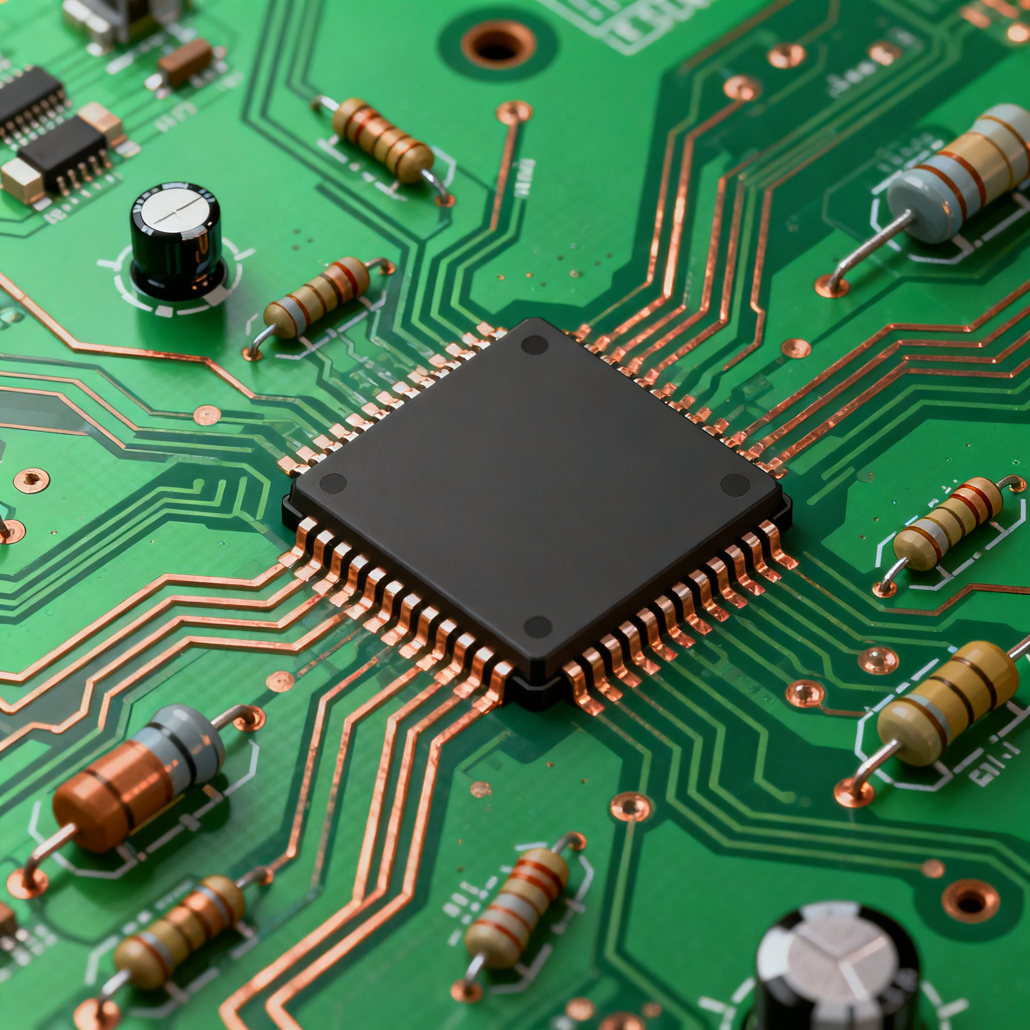
The core of any electronic device lies in its integrated circuits, which function as the brain of the system. These IC chips are embedded onto PCBs, facilitating communication between various components to perform specific tasks. The architecture of ICs involves a complex interplay of transistors, diodes, resistors, and capacitors, all miniaturized onto a silicon substrate. Key principles such as Moore's Law, which predicts the doubling of transistors on a chip approximately every two years, drive the continual advancement in IC technology. This growth necessitates meticulous attention to design and specification details to ensure optimal performance and cost-effectiveness.
Understanding the architecture of ICs helps engineers make informed decisions regarding the selection and integration of these components into PCBs. Factors such as CPU speed, memory capacity, power consumption, and peripheral support directly influence the efficiency and functionality of the final product. Furthermore, adherence to industry standards, such as those set by the IPC, ensures quality and reliability in PCB manufacturing. By aligning design practices with these standards, manufacturers can achieve competitive advantages in both performance and cost.
Detailed Specifications
When selecting IC chips for PCB applications, certain specifications are paramount. These include CPU speed, memory size, available peripherals, power requirements, and package type. Understanding these elements helps in choosing the right components that align with the intended application, ensuring both performance and cost-efficiency. Below is a detailed table outlining core specifications of typical IC chips used in PCB manufacturing.
| Specification | Details | Significance |
|---|---|---|
| CPU Speed | 1.2 GHz | Determines processing capacity and speed |
| Memory | 512 MB RAM | Influences data handling and multitasking ability |
| Peripherals | USB, I2C, SPI | Enables connectivity with other devices |
| Power Consumption | 5V, 200mA | Affects energy efficiency and battery life |
| Package Type | QFN | Impacts size and soldering technique |
| Operating Temperature | -40 to 85°C | Defines environmental resilience |
| Flash Memory | 256 KB | Stores firmware and essential data |
| ADC Resolution | 12-bit | Determines the precision of analog inputs |
| PWM Channels | 4 | Controls motor speed and LED brightness |
| Package Size | 7x7 mm | Influences board layout and component density |
Key Takeaways from the Specifications
The core specifications of an IC chip provide critical insights into its capabilities and limitations. CPU speed and memory are pivotal, dictating the processing power and efficiency of the system. Peripherals such as USB, I2C, and SPI determine the chip's ability to interface with other components, essential for creating versatile applications. Power consumption is crucial for battery-operated devices, where efficiency directly impacts operational longevity. Understanding these specifications allows engineers to select components that best align with their design goals and constraints, ensuring optimal performance and cost-effectiveness.
| Characteristic | Value | Impact |
|---|---|---|
| Operating Voltage | 3.3V | Determines power supply requirements |
| Max Current | 100 mA | Influences power distribution design |
| Clock Speed | 50 MHz | Affects processing speed and timing |
| Input Voltage Range | 0-5V | Defines compatibility with other components |
| Output Current | 20 mA per pin | Limits the load each pin can drive |
| ESD Protection | 2 kV | Prevents electrostatic damage |
| Rise/Fall Time | 5 ns | Impacts signal integrity and performance |
| I/O Voltage Levels | TTL | Determines interfacing standards |
| Leakage Current | 1 µA | Affects power efficiency in standby mode |
| Impedance | 50 Ohms | Influences signal transmission quality |
Practical Implications
The electrical characteristics of IC chips are crucial for ensuring reliable operation within a PCB. Operating voltage and current ratings dictate the power supply design and thermal management strategies. Clock speed and timing parameters influence the overall performance and synchronization of the system. Additionally, ESD protection and leakage current considerations are vital for enhancing robustness and energy efficiency. By understanding these electrical characteristics, engineers can design PCBs that not only meet performance requirements but also adhere to safety and regulatory standards.
| Use Case | Configuration | Benefits |
|---|---|---|
| Consumer Electronics | High-speed CPU, Low power | Enhanced user experience, longer battery life |
| Industrial Automation | Robust I/O, High reliability | Improved process control, reduced downtime |
| Automotive Systems | High temperature tolerance, Safety features | Increased safety, operational efficiency |
| Medical Devices | Precision ADC, Low noise | Accurate diagnostics, patient safety |
| IoT Devices | Wireless connectivity, Energy-efficient | Seamless integration, extended operational time |
| Telecommunications | High bandwidth, Low latency | Faster data transmission, improved connectivity |
| Wearable Technology | Compact size, Low power | Portability, extended usage time |
Application Guidelines
Selecting the right IC configuration for your application can significantly impact the performance and cost-efficiency of your product. For consumer electronics, prioritizing high-speed processing and low power consumption enhances user satisfaction and device longevity. In industrial automation, robust I/O configurations and high reliability are essential for maintaining operational efficiency. Medical devices benefit from precision ADCs and low noise levels, ensuring accurate diagnostics. By aligning component selection with specific application requirements, engineers can optimize both functionality and cost, leading to successful product deployment.
Design Considerations
Designing PCBs with cost optimization in mind requires a strategic approach that balances performance, reliability, and budget constraints. Key considerations include:
- Component Selection: Choose components that offer the best balance between cost and performance. Utilize datasheets and manufacturer recommendations to ensure compatibility and efficiency.
- PCB Layout: Optimize the layout for minimal signal interference and efficient power distribution. Adhering to IPC design standards can help achieve this.
- Thermal Management: Implement effective heat dissipation techniques, such as heat sinks and thermal vias, to maintain component performance and longevity.
- Test and Validation: Conduct thorough testing to validate the design and identify potential issues before mass production.
- Supply Chain Management: Establish relationships with reliable suppliers to ensure component availability and cost stability.
- Regulatory Compliance: Ensure the design meets relevant industry standards and regulations, such as RoHS and CE, to avoid legal and market entry issues.
Step-by-Step Implementation
- Define Requirements: Clearly outline the performance, cost, and regulatory requirements for the PCB.
- Select Components: Use datasheets and selection criteria to choose appropriate IC chips and other components.
- Create Schematic: Design the circuit schematic using PCB design software, ensuring all connections are logically and electrically correct.
- Design PCB Layout: Develop the PCB layout, focusing on minimizing trace lengths and optimizing component placement for signal integrity.
- Prototype and Test: Fabricate a prototype PCB and conduct functional and performance testing to identify and rectify any issues.
- Iterate Design: Based on test results, refine the design to address any identified weaknesses or inefficiencies.
- Finalize Design: Once testing confirms the design meets all requirements, finalize the design for mass production.
- Production and Quality Control: Oversee the manufacturing process and implement quality control measures to ensure consistent product quality.
Common Issues & Solutions
- Signal Integrity Problems: Use proper grounding techniques and layout strategies to reduce interference and signal degradation.
- Thermal Management Challenges: Incorporate thermal vias and heat sinks to effectively dissipate heat.
- Component Availability: Maintain a diverse supplier network to mitigate risks associated with component shortages.
- Cost Overruns: Regularly review and optimize the bill of materials to keep costs within budget.
- Regulatory Non-Compliance: Stay informed about regulatory changes and integrate compliance checks into the design process.
- Design Flaws: Implement a robust design review and testing process to catch and correct errors early.
Applications & Use Cases
PCBs with optimized IC chip integration find applications across various industries. In consumer electronics, they enhance device performance and efficiency, leading to better user experiences. Industrial automation systems benefit from improved process control and reliability. In the automotive sector, they contribute to vehicle safety and operational efficiency. Medical devices leverage precise data handling for accurate diagnostics. Telecommunications and IoT applications see improvements in connectivity and data transmission. By tailoring PCB designs to specific use cases, manufacturers can deliver products that meet market demands and customer expectations.
Selection & Sourcing Guide
For engineers looking to source IC chips and other components, IC Online offers a comprehensive platform for component selection and procurement. By leveraging such resources, engineers can access a wide range of components, ensuring they find the right fit for their projects while maintaining cost-effectiveness and availability.
FAQ
- What are the key factors in selecting an IC chip? Consider CPU speed, memory, power consumption, and peripheral support.
- How does component selection impact PCB cost? Choosing cost-effective components without compromising performance can significantly reduce overall costs.
- What are common pitfalls in PCB design? Signal integrity issues, thermal management failures, and regulatory non-compliance are common challenges.
- How can I ensure regulatory compliance in my design? Adhere to industry standards such as IPC and stay informed about regulatory updates.
- What role does thermal management play in PCB design? Effective thermal management ensures component reliability and longevity by preventing overheating.
- How do I optimize my PCB layout? Focus on minimizing trace lengths, optimizing component placement, and ensuring proper grounding.
- What testing procedures should I implement? Conduct functional, performance, and environmental testing to validate the design.
- How can I mitigate component availability risks? Establish strong supplier relationships and maintain a diverse network of component sources.
- What is the importance of datasheets in component selection? Datasheets provide essential specifications and guidelines for proper component integration.
- How do I balance performance and cost in my design? Prioritize components that offer the best performance-to-cost ratio and leverage design optimization techniques.
Conclusion
Optimizing the PCB manufacturing process requires a thorough understanding of component specifications, electrical characteristics, and application requirements. By carefully selecting IC chips and adhering to industry best practices, engineers can achieve cost-effective designs that meet performance and regulatory standards. This comprehensive guide provides a roadmap for navigating the complexities of PCB design and manufacturing, ensuring successful product development in 2026 and beyond.