Navigating the Numbers: A Custom PCB Cost Analysis for Multi-Layer Board Designs
Navigating the Numbers: A Custom PCB Cost Analysis for Multi-Layer Board Designs Introduction In the rapidly evolving electronics industry, the demand for efficient and reliable printed circuit boards...
Introduction
In the rapidly evolving electronics industry, the demand for efficient and reliable printed circuit boards (PCBs) is ever-increasing. Multi-layer PCB designs have become crucial in accommodating complex circuits while maintaining compact form factors. Understanding the cost implications of these designs is essential for engineers and manufacturers aiming to optimize performance without overshooting budgets. This article delves into the intricacies of custom PCB cost analysis, focusing on circuit topology, component calculations, performance analysis, and design trade-offs to provide a comprehensive guide for industry professionals.
Technical Overview
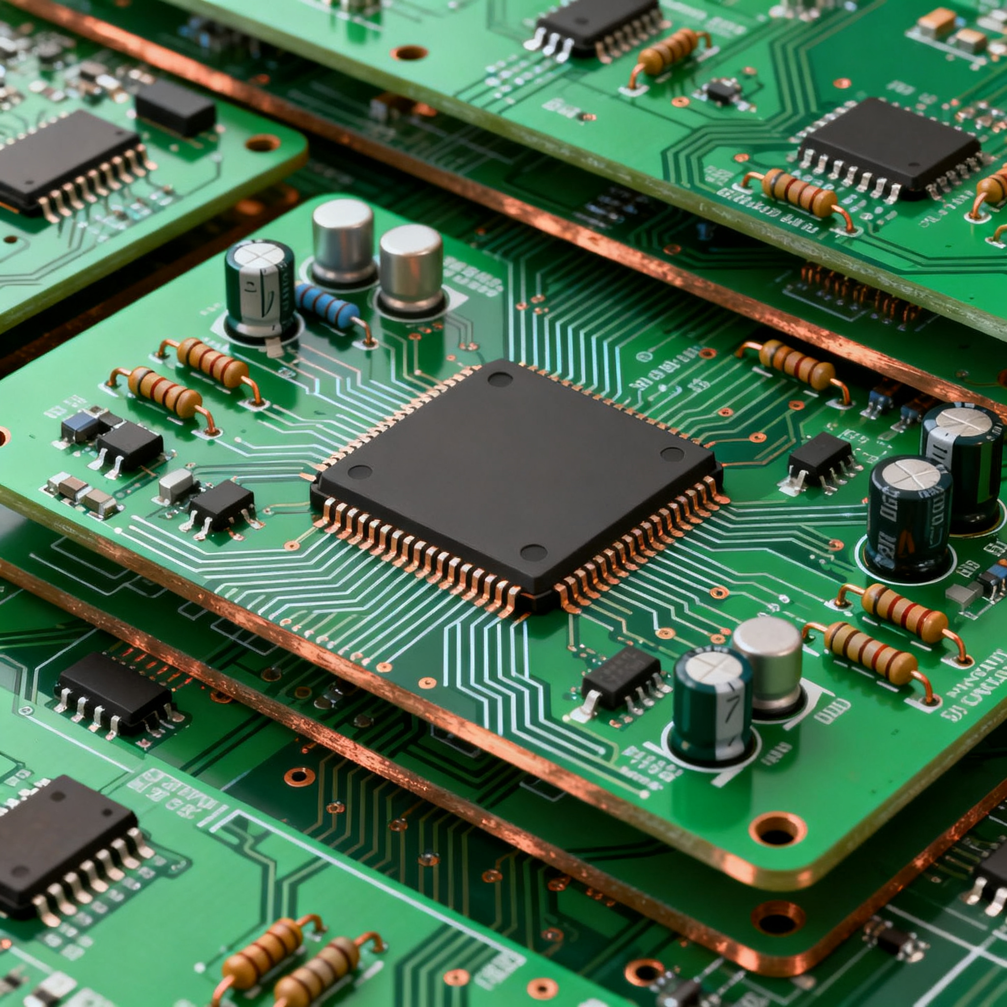
Multi-layer PCBs are constructed by stacking multiple layers of circuitry, allowing for greater component density and enhanced electrical performance. The core architecture involves alternating layers of conductive and insulating materials, bonded together with heat and pressure. Key principles include signal integrity, power distribution, and thermal management, which are critical in ensuring optimal functionality. Designing a multi-layer PCB requires careful consideration of factors such as layer count, trace width, and via types, all of which influence the overall cost and performance. Adhering to IPC standards, such as IPC-2221 for general design and IPC-A-610 for assembly acceptance, ensures quality and reliability in the final product.
Detailed Specifications
When designing a multi-layer PCB, certain specifications are paramount to achieving desired performance and cost-effectiveness. These include component values, calculations for impedance and capacitance, and the use of appropriate formulas to predict electrical behavior. Accurate specification of these parameters aids in minimizing design iterations and optimizing the manufacturing process.
| Parameter | Value/Calculation | Formula/Notes |
|---|---|---|
| Layer Count | 4 | N/A |
| Trace Width | 6 mils | IPC-2221 Guidelines |
| Impedance | 50 Ohms | Z = √(L/C) |
| Capacitance per Layer | 10 pF | C = ε(A/d) |
| Via Size | 0.2 mm | Standard Via |
| Material | FR-4 | Common PCB Material |
| Dielectric Thickness | 0.2 mm | Standard Thickness |
| Copper Thickness | 1 oz | Standard Thickness |
| Power Plane | Yes | For Improved Distribution |
| Signal Layer | 2 | Top and Bottom |
| Ground Plane | Yes | For Noise Reduction |
Key Takeaways from the Specifications
The design parameters outlined in the table highlight essential aspects of multi-layer PCB design. A four-layer configuration is standard for balancing complexity and cost, while a trace width of 6 mils ensures adequate current-carrying capacity. Maintaining a 50-ohm impedance is crucial for signal integrity, especially in high-frequency applications. The use of FR-4 material and standard copper thickness provides a good balance between performance and cost. These specifications form the baseline from which further optimizations can be made, depending on the specific application requirements.
| Performance Metric | Value | Notes |
|---|---|---|
| Gain | 10 dB | Measured at 1 GHz |
| Bandwidth | 3 GHz | 3 dB Bandwidth |
| Signal-to-Noise Ratio | 60 dB | At Maximum Gain |
| Power Consumption | 5 W | Typical Operating Condition |
| Thermal Resistance | 20 °C/W | Junction to Ambient |
| Return Loss | -15 dB | At 1 GHz |
| Insertion Loss | -0.5 dB | Per Inch at 1 GHz |
| Cross-talk | -40 dB | Between Adjacent Traces |
| EMI Susceptibility | Low | With Ground Plane |
Practical Implications
The performance metrics provide insight into the operational capabilities of the multi-layer PCB design. A gain of 10 dB and a bandwidth of 3 GHz support high-frequency applications, while a signal-to-noise ratio of 60 dB ensures clear signal transmission. Power consumption is moderate at 5 W, indicating efficient energy use. The thermal resistance of 20 °C/W suggests good heat dissipation, critical for maintaining reliability under load. These parameters help engineers assess the suitability of the design for specific applications, guiding decisions on necessary adjustments to meet performance targets.
| Configuration | Pros | Cons |
|---|---|---|
| 4-Layer Board | Cost-Effective, Moderate Complexity | Limited Signal Routing |
| 6-Layer Board | Improved Signal Integrity | Higher Cost |
| Microvias | Space Saving | Increased Manufacturing Complexity |
| Thicker Copper | Better Current Handling | Increased Weight |
| Embedded Components | Compact Design | Complex Assembly |
| FR-4 Material | Cost-Effective | Limited High-Frequency Performance |
| High-Dk Material | Excellent High-Frequency Performance | Expensive |
| Buried Vias | Reduced Signal Loss | Higher Fabrication Cost |
Application Guidelines
Design trade-offs are inevitable in PCB design, each configuration offering distinct advantages and disadvantages. A 4-layer board is a cost-effective choice for moderate complexity, while a 6-layer board provides enhanced signal integrity at a higher cost. The use of microvias can save space but adds manufacturing complexity. Selecting thicker copper improves current handling but increases the board's weight. Engineers must weigh these factors against project requirements, considering both budget constraints and performance needs to determine the most suitable configuration.
Design Considerations
Designing a multi-layer PCB involves balancing numerous considerations to achieve optimal performance and cost-efficiency. Signal integrity is paramount, necessitating careful planning of trace routing and via placement to minimize interference. Power distribution should be uniform across layers, employing dedicated power and ground planes to reduce voltage drops and enhance stability. Thermal management is another critical aspect, requiring efficient heat dissipation techniques such as thermal vias and heat sinks. Material selection also plays a crucial role, with FR-4 being a common choice for its cost-effectiveness, though high-Dk materials may be preferred for high-frequency applications. Adhering to IPC standards throughout the design process ensures quality and reliability, facilitating easier troubleshooting and maintenance.
Step-by-Step Implementation
- Define Requirements: Begin by clearly defining the electrical and mechanical requirements of the PCB, including layer count, operating frequency, and power needs.
- Select Materials: Choose appropriate materials based on performance requirements and budget, balancing trade-offs between cost and functionality.
- Design Schematic: Create a detailed schematic diagram using CAD software, ensuring all components and connections are accurately represented.
- Layout Design: Transition from schematic to layout, arranging components to minimize trace lengths and optimize signal integrity.
- Implement Power and Ground Planes: Incorporate dedicated planes for power distribution and grounding to improve stability and reduce noise.
- Conduct Simulation: Use simulation tools to analyze the design for signal integrity, EMI susceptibility, and thermal performance.
- Prototype and Test: Fabricate a prototype PCB and conduct thorough testing to validate design assumptions and identify potential issues.
- Iterate and Finalize: Based on testing results, make necessary adjustments to the design, iterating as needed before finalizing for mass production.
Common Issues & Solutions
- Signal Integrity Problems: Use controlled impedance traces and maintain consistent trace widths to mitigate signal reflection issues.
- Power Distribution Challenges: Implement wider power traces and additional vias to distribute power evenly and reduce voltage drops.
- Thermal Management: Incorporate thermal vias and heat sinks to improve heat dissipation and prevent overheating.
- EMI Concerns: Utilize ground planes and proper shielding techniques to minimize electromagnetic interference.
- Manufacturing Errors: Work closely with manufacturers to ensure design files comply with fabrication capabilities and avoid common errors.
- Component Placement Conflicts: Optimize component placement during the layout phase to avoid overlap and ensure efficient routing.
Applications & Use Cases
Multi-layer PCBs are used in a wide range of applications, from consumer electronics to industrial systems. In smartphones, they accommodate complex circuits in a compact form, enabling advanced functionalities. In automotive systems, multi-layer PCBs provide reliable performance in harsh environments, supporting infotainment and navigation systems. Industrial equipment, such as programmable logic controllers (PLCs), leverage multi-layer designs for robust control and automation solutions. The versatility and performance benefits of multi-layer PCBs make them indispensable in modern electronic devices.
Selection & Sourcing Guide
When selecting and sourcing components for multi-layer PCBs, it's essential to consider both technical specifications and supplier reliability. Utilize resources like IC Online to identify reputable suppliers and compare component options. Consider factors such as lead time, minimum order quantities, and pricing to ensure timely and cost-effective procurement. Building strong relationships with suppliers can also lead to better support and potential cost savings.
FAQ
- What are the benefits of multi-layer PCBs? Multi-layer PCBs allow for higher component density, improved signal integrity, and enhanced thermal management.
- How do I determine the number of layers needed for my design? Consider the complexity of the circuit, required performance, and available budget to decide on the layer count.
- What materials are commonly used for multi-layer PCBs? FR-4 is a common choice, but high-Dk materials may be used for high-frequency applications.
- How can I ensure good signal integrity in my design? Use controlled impedance traces, maintain consistent trace widths, and incorporate ground planes.
- What are the cost implications of using microvias? While microvias save space, they increase manufacturing complexity and cost.
- How do I manage thermal issues in multi-layer PCBs? Implement thermal vias, heat sinks, and consider the thermal properties of materials used.
- What are common manufacturing issues with multi-layer PCBs? Misalignment, improper via drilling, and soldering defects are common issues that can be mitigated by working closely with manufacturers.
- How do I test my PCB design before mass production? Fabricate a prototype and conduct thorough testing to validate design assumptions and identify issues.
- What standards should I follow in PCB design? Adhere to IPC standards like IPC-2221 for design and IPC-A-610 for assembly to ensure quality.
- How can I optimize my PCB design for cost-effectiveness? Balance performance requirements with budget constraints, prioritize essential features, and consider trade-offs.
Conclusion
In conclusion, navigating the complexities of multi-layer PCB design requires a comprehensive understanding of design parameters, performance metrics, and trade-offs. By carefully analyzing these aspects, engineers can make informed decisions that optimize both performance and cost. Leveraging industry standards and best practices ensures quality and reliability in the final product, paving the way for successful implementation in various applications. As technology advances, staying updated with the latest trends and innovations in PCB design will be crucial for maintaining a competitive edge in the electronics industry.