Navigating PCB Production Lead Times: Strategies for Timely Deliveries
Navigating PCB Production Lead Times: Strategies for Timely Deliveries table { border-collapse: collapse; width: 100%; margin: 20px 0; } th, td { border: 1px solid #000; padding: 8px; } thead tr { bac...
Introduction
In the rapidly evolving electronics industry, timely delivery of printed circuit boards (PCBs) is crucial for maintaining competitive advantage. As the backbone of electronic devices, PCBs must be designed and produced efficiently to meet market demands. Navigating production lead times involves understanding design rules, stackup configurations, signal integrity, and manufacturing processes. This article explores strategies to ensure timely PCB deliveries, drawing on industry standards and best practices.
Technical Overview
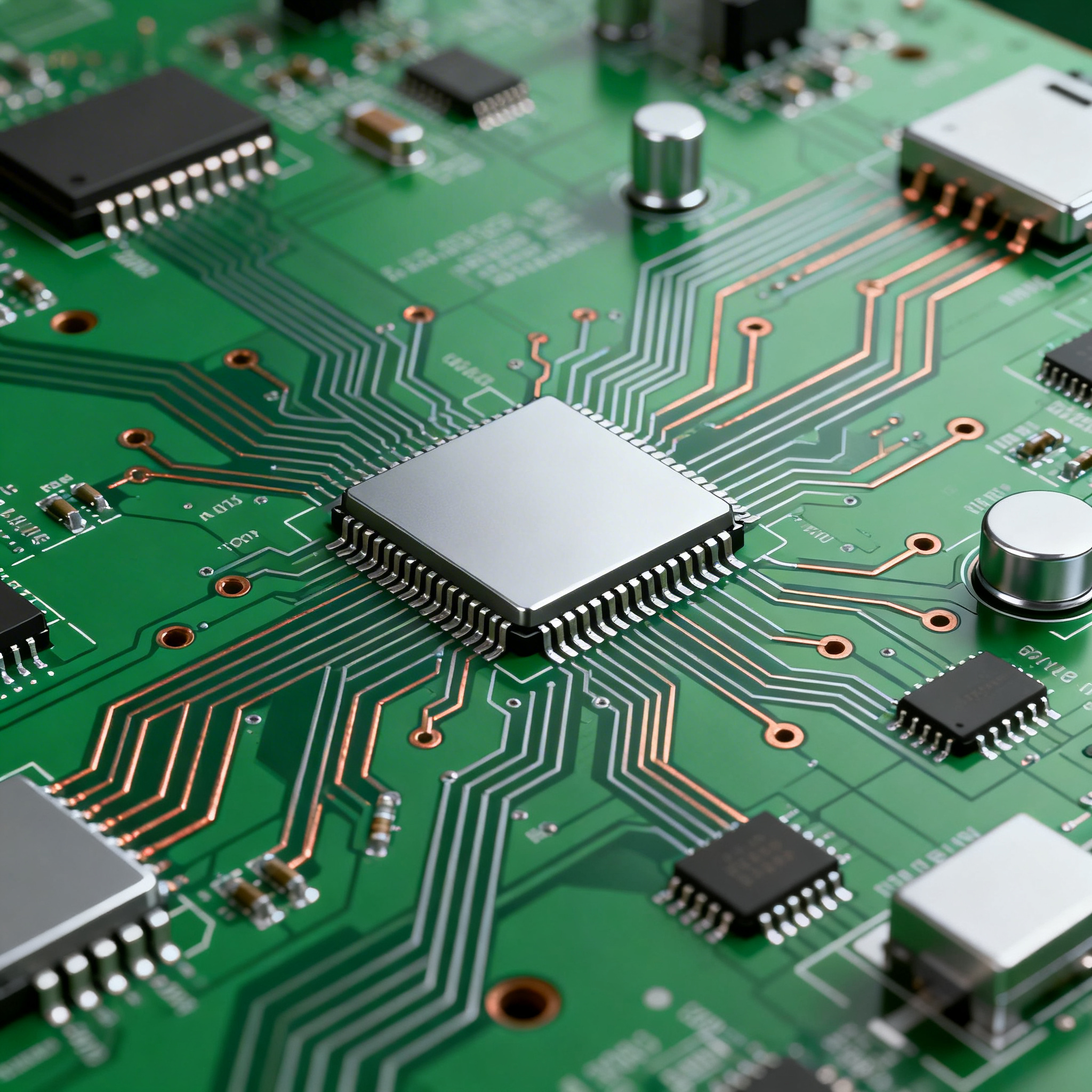
PCBs are integral to electronic devices, serving as the foundation for mounting and interconnecting components. The design and production of PCBs involve several critical considerations, including layout rules, layer stackup, and signal integrity. Compliance with industry standards, such as those set by the IPC, ensures quality and reliability. Understanding these principles allows for optimized designs that reduce production lead times and enhance performance.
Detailed Specifications
Effective PCB production begins with adhering to design specifications that guide the layout and fabrication processes. Key specifications include trace width, spacing, via sizes, and clearances, which ensure electrical performance and manufacturability. Below is a table detailing essential PCB design rules.
| Parameter | Minimum Value | Description |
|---|---|---|
| Trace Width | 6 mil | Minimum width for signal traces to ensure current capacity and integrity |
| Trace Spacing | 6 mil | Minimum spacing between traces to prevent short circuits |
| Via Size | 10 mil | Minimum diameter for vias to ensure manufacturability and reliability |
| Via Hole Size | 8 mil | Minimum hole size for vias to accommodate plating and connectivity |
| Pad Size | 20 mil | Minimum size for component pads to ensure solderability |
| Annular Ring | 4 mil | Minimum width of the ring around via holes for reliable connection |
| Clearance to Edge | 10 mil | Minimum distance from traces to board edge to prevent damage |
| Component Clearance | 50 mil | Minimum spacing between components to facilitate assembly |
| Silkscreen Clearance | 4 mil | Minimum distance between silkscreen and pads/traces to prevent interference |
| Board Thickness | 1.6 mm | Standard thickness for mechanical strength and compatibility |
| Aspect Ratio | 8:1 | Maximum ratio of board thickness to smallest hole diameter for reliable plating |
Key Takeaways from the Specifications
The specifications outlined in the table are critical for ensuring the manufacturability and performance of PCBs. Adhering to these design rules minimizes the risk of defects and reduces production delays. For instance, maintaining proper trace width and spacing is essential for signal integrity and preventing electrical shorts. Similarly, appropriate via sizes and annular rings ensure reliable interconnections. Understanding these parameters allows designers to create layouts that meet both electrical and mechanical requirements, facilitating smoother manufacturing processes.
| Layer Configuration | Number of Layers | Typical Applications |
|---|---|---|
| Single Layer | 1 | Simple circuits, low-cost consumer electronics |
| Double Layer | 2 | Consumer electronics, basic industrial devices |
| Four Layer | 4 | Compact devices, basic computing equipment |
| Six Layer | 6 | Advanced computing, communication devices |
| Eight Layer | 8 | High-performance computing, RF applications |
| Ten Layer | 10 | Complex systems, high-density interconnects |
| Twelve Layer | 12 | Advanced telecommunications, aerospace |
| Sixteen Layer | 16 | Military, high-frequency applications |
Practical Implications
The layer stackup options presented in the table highlight the versatility of PCB designs for various applications. Single and double-layer boards are prevalent in low-cost and simple devices, while multi-layer configurations cater to more complex systems requiring higher density and performance. Selecting the appropriate layer configuration is crucial for achieving the desired balance between functionality, cost, and manufacturability. For instance, a four-layer board might be optimal for compact devices, offering improved signal integrity and reduced electromagnetic interference.
| Material | Dielectric Constant (Dk) | Loss Tangent (Df) |
|---|---|---|
| FR-4 | 4.5 | 0.02 |
| Rogers 4350B | 3.48 | 0.0037 |
| Rogers 4003C | 3.55 | 0.0027 |
| Isola FR408HR | 3.68 | 0.009 |
| Nelco N4000-13 | 3.7 | 0.016 |
| Arlon 85N | 3.5 | 0.004 |
| Panasonic Megtron 6 | 3.7 | 0.004 |
| Ventec VT-47 | 4.2 | 0.008 |
| Polyimide | 4.2 | 0.01 |
| PTFE | 2.2 | 0.001 |
Application Guidelines
The selection of materials for PCB fabrication significantly impacts signal integrity and overall performance. The table provides a comparison of common materials, highlighting their dielectric constants and loss tangents. FR-4 is a widely used material due to its balance of performance and cost, suitable for general applications. For high-frequency and RF applications, materials like Rogers and PTFE offer lower dielectric constants and loss tangents, ensuring minimal signal loss. Understanding these properties helps in selecting the right material based on application requirements and performance criteria.
Design Considerations
Designing a PCB involves several considerations to ensure functionality and manufacturability. Key factors include adhering to industry standards, optimizing layout for signal integrity, and selecting appropriate materials. Designers should prioritize trace width and spacing to prevent electrical shorts and ensure current capacity. Additionally, the choice of stackup configuration influences signal integrity and electromagnetic compatibility. Material selection is also critical, as it affects thermal management and mechanical durability. By aligning design choices with manufacturing capabilities, engineers can streamline production and reduce lead times.
Step-by-Step Implementation
Implementing a successful PCB design involves a systematic approach:
- Define Requirements: Clearly outline the functional and performance requirements of the PCB, including electrical, mechanical, and environmental specifications.
- Choose Materials: Select appropriate materials based on dielectric properties, thermal performance, and cost considerations.
- Design Schematic: Create a detailed schematic capturing all electrical connections and components.
- Layout Design: Translate the schematic into a physical layout, adhering to design rules for trace width, spacing, and via placement.
- Simulate Performance: Use simulation tools to analyze signal integrity, power distribution, and thermal characteristics.
- Review and Validate: Conduct design reviews and validate against industry standards and requirements.
- Prepare for Manufacturing: Generate fabrication and assembly files, including Gerber files and bill of materials.
- Collaborate with Manufacturers: Work closely with fabrication and assembly partners to address potential issues and optimize production processes.
Common Issues & Solutions
Designing and manufacturing PCBs can present several challenges. Here are five common issues and their solutions:
- Signal Integrity Problems: Use proper trace width and spacing, and employ differential pairs for high-speed signals.
- Thermal Management: Implement thermal vias and pads, and consider using heat sinks or thermal interface materials.
- Component Placement Conflicts: Ensure adequate clearance and orientation during the layout design phase.
- Manufacturing Defects: Adhere to IPC standards and conduct thorough design reviews to catch errors early.
- Cost Overruns: Optimize design for manufacturability and consider economies of scale in material selection and production.
Applications & Use Cases
PCBs are ubiquitous in modern electronics, with applications ranging from consumer gadgets to industrial systems. In telecommunications, multi-layer PCBs enable high-speed data processing and signal routing. In automotive electronics, PCBs support advanced driver-assistance systems (ADAS) and infotainment. The medical field relies on PCBs for diagnostic and monitoring equipment, where precision and reliability are paramount. Each application demands specific design considerations to meet performance and regulatory standards.
Selection & Sourcing Guide
When selecting and sourcing PCB components, it's essential to consider suppliers with a proven track record of quality and reliability. Utilize platforms like IC Online for sourcing components, ensuring compatibility with design specifications and lead time requirements. Collaborating with reputable manufacturers and suppliers can streamline the production process and reduce delays.
FAQ
- What is the typical lead time for PCB production? Lead times vary based on complexity and volume but typically range from a few days to several weeks.
- How can I reduce PCB production lead times? Optimize design for manufacturability, select materials wisely, and collaborate closely with manufacturers.
- What are the key factors affecting PCB cost? Material selection, layer count, and complexity are major cost drivers.
- How do I ensure signal integrity in my PCB design? Use proper trace routing, maintain impedance control, and minimize crosstalk.
- What is the role of IPC standards in PCB design? IPC standards ensure quality, reliability, and consistency in PCB fabrication and assembly.
- What should I consider when selecting PCB materials? Consider dielectric properties, thermal performance, and application-specific requirements.
- Can I use multiple materials in a single PCB? Yes, hybrid designs can incorporate different materials to optimize performance for specific applications.
- How do I handle thermal management in PCBs? Use thermal vias, proper component placement, and heat sinks to manage heat dissipation.
- What tools are available for PCB design simulation? Tools like Altium Designer, Cadence Allegro, and Mentor Graphics offer comprehensive simulation capabilities.
- How do I verify my PCB design before manufacturing? Conduct design reviews, simulations, and compliance checks against industry standards.
Conclusion
In conclusion, navigating PCB production lead times requires a comprehensive understanding of design rules, material properties, and manufacturing processes. By adhering to industry standards, optimizing designs for manufacturability, and collaborating with reliable suppliers, engineers can ensure timely and successful PCB production. This strategic approach not only enhances performance and reliability but also provides a competitive edge in the fast-paced electronics industry.