Multilayer PCB Stack-Up Design: Cost Optimization Tips for Enhanced Performance and Efficiency
Introduction In the world of electronics, multilayer PCB stack-up design is a crucial element that significantly impacts the performance and efficiency of electronic devices. As the demand for compact...
Introduction
In the world of electronics, multilayer PCB stack-up design is a crucial element that significantly impacts the performance and efficiency of electronic devices. As the demand for compact, high-performance electronics continues to rise, the need for optimized PCB designs becomes paramount. This article delves into the intricacies of multilayer PCB stack-up design, focusing on cost optimization tips to enhance both performance and efficiency. By understanding the core specifications, electrical characteristics, and application comparisons, designers can make informed decisions that lead to superior product outcomes.
Technical Overview
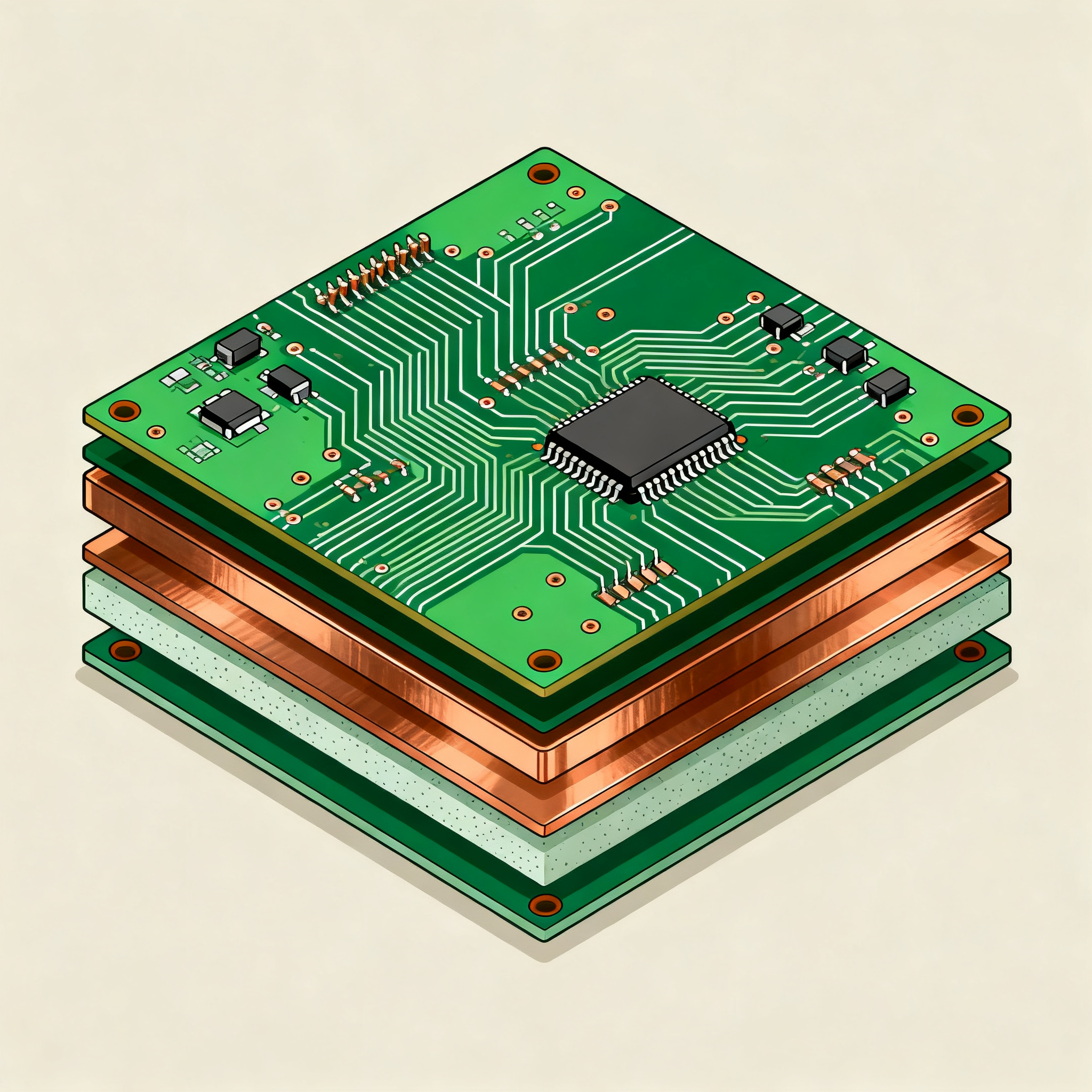
Multilayer PCB stack-up design involves the arrangement of multiple layers of circuitry within a single PCB. Each layer has a specific function, such as power distribution, signal routing, or grounding. The stack-up configuration plays a pivotal role in determining the electrical performance, thermal management, and mechanical stability of the PCB. Key principles include minimizing signal interference, optimizing thermal paths, and ensuring mechanical integrity. The architecture of a multilayer PCB typically includes core materials, copper layers, dielectric materials, and solder masks. By adhering to IPC standards and leveraging resources from PCB manufacturers, designers can achieve optimal results.
Detailed Specifications
When designing multilayer PCBs, understanding the component specifications is essential. Key specifications include CPU speed, memory, peripherals, power requirements, and package types. These specifications determine the overall capability and compatibility of the PCB with the intended application. By analyzing datasheets and selecting components that meet the desired criteria, designers can optimize the PCB design for performance and cost efficiency.
| Specification | Details | Significance |
|---|---|---|
| CPU Speed | 1.2 GHz | Determines processing power and efficiency |
| Memory | 4 GB DDR4 | Influences multitasking capabilities |
| Peripherals | USB, HDMI, Ethernet | Defines connectivity options |
| Power | 5V, 2A | Impacts power supply requirements |
| Package | BGA | Affects thermal and space considerations |
| Storage | 32 GB eMMC | Determines data storage capacity |
| Operating Temperature | -40°C to 85°C | Defines environmental adaptability |
| Dimensions | 90mm x 60mm | Impacts physical layout |
| Layer Count | 8 Layers | Affects signal integrity and cost |
| Material | FR-4 | Commonly used for its balance of cost and performance |
Key Takeaways from the Specifications
The specifications outlined in Table 1 provide a comprehensive overview of the core attributes essential for a high-performance PCB design. CPU speed and memory are critical for processing and multitasking capabilities, while peripherals like USB and HDMI determine the device's connectivity options. Power requirements influence the design of power supply circuits, and the package type impacts both thermal management and space utilization. Understanding these specifications allows designers to tailor PCB designs to meet specific application needs while optimizing for cost and performance.
| Characteristic | Value | Significance |
|---|---|---|
| Operating Voltage | 3.3 V | Determines power consumption and compatibility |
| Current Consumption | 500 mA | Impacts battery life and power supply design |
| Input Voltage Range | 2.7 V - 5.5 V | Defines flexibility in power source |
| Output Current | 250 mA | Determines load capacity |
| Signal Rise Time | 2 ns | Affects signal integrity and speed |
| Input Impedance | 50 Ohms | Influences signal reflection and transmission |
| Output Impedance | 75 Ohms | Impacts signal strength and quality |
| Switching Frequency | 1 MHz | Affects efficiency and noise |
| Propagation Delay | 5 ns | Influences timing and synchronization |
| Thermal Resistance | 35°C/W | Determines thermal management needs |
| Leakage Current | 10 µA | Impacts long-term reliability |
Practical Implications
The electrical characteristics in Table 2 provide insights into the operational parameters of the PCB. Operating voltage and current consumption are crucial for designing efficient power supplies and ensuring battery longevity. Signal rise time and propagation delay are vital for maintaining signal integrity and ensuring accurate timing. Thermal resistance is a critical factor in managing heat dissipation, especially in high-density designs. By understanding these characteristics, designers can make informed decisions to enhance performance and reliability while minimizing power consumption and thermal issues.
| Application | Configuration | Benefits |
|---|---|---|
| Consumer Electronics | 4-layer stack-up | Cost-effective and compact design |
| Automotive Systems | 8-layer stack-up | Enhanced thermal management and reliability |
| Industrial Control | 6-layer stack-up | Improved signal integrity and durability |
| Medical Devices | 10-layer stack-up | High precision and safety features |
| Telecommunications | 12-layer stack-up | Advanced signal processing capabilities |
| Aerospace Applications | 16-layer stack-up | Superior performance in extreme conditions |
Application Guidelines
The application comparison in Table 3 highlights the versatility of multilayer PCB stack-up designs across various industries. Consumer electronics benefit from cost-effective 4-layer designs, while automotive systems require more complex 8-layer configurations for better thermal management. Medical devices demand high precision and safety, achievable with a 10-layer stack-up. Each application has unique requirements, and selecting the appropriate stack-up configuration is crucial for optimizing performance, reliability, and cost. By aligning the stack-up design with the specific needs of the application, designers can ensure successful product implementation.
Design Considerations
When designing multilayer PCBs, several considerations must be taken into account to achieve optimal performance and cost efficiency. First, the selection of materials is crucial; FR-4 is commonly used for its balance of cost and performance, but high-frequency applications may require specialized materials. The layer count significantly impacts both the cost and signal integrity, with more layers offering better performance but at a higher cost. It is essential to balance these factors based on the application requirements.
Signal integrity is another critical consideration. Proper layer stack-up and routing techniques can minimize interference and reflection, ensuring clean signal transmission. Ground and power planes should be strategically placed to provide stable voltage references and reduce electromagnetic interference (EMI).
Thermal management is vital in preventing overheating and ensuring long-term reliability. Implementing thermal vias, heat sinks, and careful component placement can effectively dissipate heat. Designers should also consider the manufacturability of the PCB design, adhering to IPC standards and manufacturer capabilities to ensure cost-effective production and assembly.
Step-by-Step Implementation
- Define the application requirements and constraints, including performance, cost, and environmental conditions.
- Select appropriate materials for the PCB, considering factors like frequency, thermal performance, and budget.
- Determine the optimal layer count, balancing performance needs with cost constraints.
- Design the layer stack-up, ensuring proper placement of power, ground, and signal layers to minimize interference and improve integrity.
- Route traces carefully, adhering to design rules for width, spacing, and via placement to ensure signal quality and manufacturability.
- Implement thermal management strategies, such as thermal vias and heat sinks, to manage heat dissipation effectively.
- Validate the design against IPC standards and perform simulations to ensure compliance and performance.
- Collaborate with the PCB manufacturer to optimize the design for production, considering their capabilities and recommendations.
Common Issues & Solutions
- Signal Integrity Issues: Use proper grounding and shielding techniques to reduce interference and reflections.
- Thermal Management Problems: Implement thermal vias and heat sinks to improve heat dissipation.
- Manufacturability Challenges: Collaborate with manufacturers to ensure design rules are met and optimize for production.
- Cost Overruns: Balance layer count and material selection to achieve a cost-effective design without compromising performance.
- EMI Concerns: Design with proper spacing and grounding to minimize electromagnetic interference.
- Component Selection: Ensure components are compatible with the PCB design and meet application requirements.
Applications & Use Cases
Multilayer PCBs are widely used across various industries due to their ability to support complex circuitry in a compact form factor. In consumer electronics, they enable the development of compact and feature-rich devices. Automotive systems benefit from improved thermal management and reliability, essential for safety-critical applications. In industrial control, multilayer PCBs enhance signal integrity and durability, crucial for harsh environments. Medical devices require precision and safety features, achievable with advanced stack-up designs. Telecommunications and aerospace applications demand superior performance, which multilayer PCBs can provide through high-layer count designs.
Selection & Sourcing Guide
When selecting and sourcing components for multilayer PCB designs, it is essential to consider factors such as performance, compatibility, and cost. Utilize resources like IC Online to research and compare components, ensuring they meet the specific requirements of your application. Collaborate with manufacturers to optimize the design for production and leverage their expertise to achieve cost-effective solutions.
FAQ
- What is a multilayer PCB? A multilayer PCB is a printed circuit board with multiple layers of circuitry stacked together to accommodate complex designs and functionalities.
- How do I choose the right layer count? Consider the application's performance, cost, and space constraints. More layers provide better performance but increase cost.
- What materials are used in multilayer PCBs? FR-4 is commonly used, but specialized materials may be required for high-frequency applications.
- How can I ensure signal integrity? Use proper grounding, shielding, and routing techniques to minimize interference and reflections.
- What are common thermal management strategies? Implement thermal vias, heat sinks, and strategic component placement to manage heat dissipation.
- How do I optimize my design for manufacturability? Collaborate with manufacturers, adhere to IPC standards, and consider their capabilities and recommendations.
- What are the benefits of multilayer PCBs in automotive systems? They offer enhanced thermal management and reliability, crucial for safety-critical applications.
- Can multilayer PCBs be used in medical devices? Yes, they provide high precision and safety features essential for medical applications.
- How do I manage cost overruns in PCB design? Balance layer count and material selection, and collaborate with manufacturers to optimize the design for cost-effectiveness.
- What are the challenges of designing multilayer PCBs? Challenges include ensuring signal integrity, thermal management, manufacturability, and cost control.
Conclusion
Multilayer PCB stack-up design is a critical aspect of modern electronics, offering enhanced performance and efficiency. By understanding core specifications, electrical characteristics, and application comparisons, designers can optimize their designs for specific applications. Careful consideration of design principles, materials, and manufacturing capabilities ensures successful implementation and cost-effective solutions. Leveraging the insights and recommendations outlined in this article will empower designers to create high-performance, reliable, and efficient multilayer PCB designs.