Maximizing Efficiency: A Step-by-Step Guide to PCB Assembly Services for Your Next Project
Maximizing Efficiency: A Step-by-Step Guide to PCB Assembly Services for Your Next Project Introduction In the rapidly evolving world of electronics, maximizing efficiency in PCB assembly services is ...
Introduction
In the rapidly evolving world of electronics, maximizing efficiency in PCB assembly services is crucial for the success of any project. As the backbone of modern electronic devices, printed circuit boards (PCBs) are essential for ensuring the functionality and reliability of products ranging from consumer electronics to industrial machinery. Understanding the intricacies of PCB assembly can significantly impact the performance and cost-effectiveness of your designs. This guide aims to provide a comprehensive overview of the core specifications, electrical characteristics, and application guidelines necessary to optimize your PCB assembly process.
Technical Overview
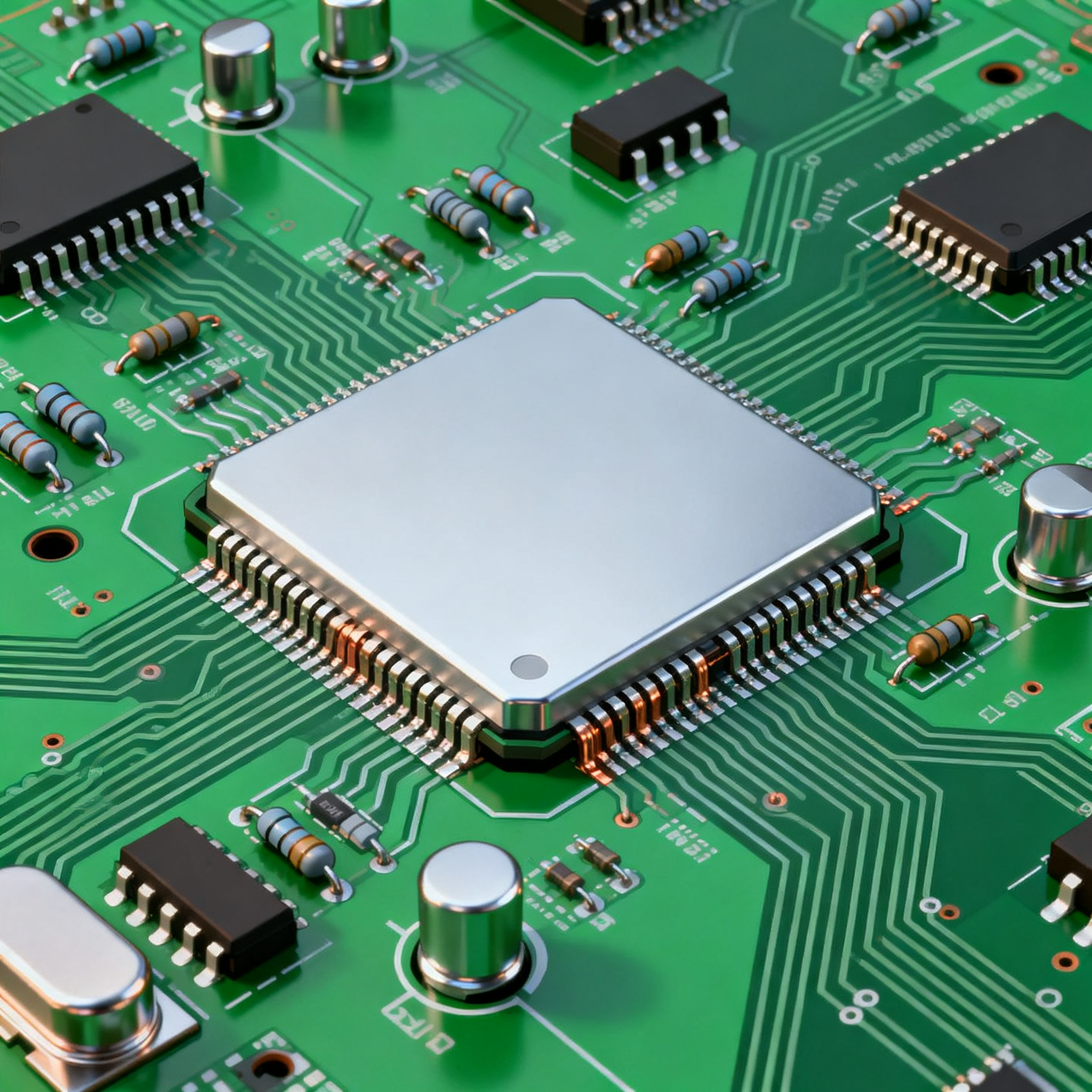
The design and assembly of PCBs involve various technical concepts and principles. At the heart of any PCB are the integrated circuits (ICs) and components that dictate its performance. The architecture of a PCB must be carefully planned to accommodate these components while ensuring signal integrity and minimizing electromagnetic interference. Key considerations include the selection of appropriate materials, layer stack-up configurations, and routing strategies. Adhering to industry standards, such as those provided by IPC, ensures quality and reliability in PCB manufacturing and assembly.
In addition to the physical design, the selection of components plays a critical role in the overall functionality of the PCB. This involves analyzing component specifications, such as CPU speed, memory capacity, and power requirements, to ensure compatibility and optimal performance. Furthermore, understanding the electrical characteristics, such as voltage levels and timing constraints, is essential for proper circuit operation. Careful consideration of these factors during the design phase can prevent costly revisions and delays in the manufacturing process.
Detailed Specifications
When embarking on a PCB assembly project, understanding the core specifications of the components you intend to use is of paramount importance. These specifications dictate the capabilities and limitations of your design, influencing everything from processing power to energy consumption. Below, we present a table outlining the critical specifications for a typical IC chip used in PCB assemblies.
| Specification | Details | Comments |
|---|---|---|
| CPU Speed | 1.2 GHz | Optimal for general-purpose applications |
| Memory | 512 MB RAM | Sufficient for basic operations |
| Peripherals | USB, I2C, SPI | Supports multiple interfaces |
| Power Consumption | 5W | Low power for energy-efficient designs |
| Package Type | LQFP | Leads for easy soldering |
| Operating Temperature | -40°C to 85°C | Suitable for industrial environments |
| Storage Capacity | 16 GB Flash | Adequate for most applications |
| GPIO Pins | 32 | Ample for various connections |
| ADC Channels | 8 | For analog signal processing |
| Dimensions | 20x20 mm | Compact design |
| Cost | $5 per unit | Economical for mass production |
Key Takeaways from the Specifications
The core specifications table provides a snapshot of the capabilities of a typical IC chip used in PCB assemblies. The CPU speed of 1.2 GHz and 512 MB of RAM make it suitable for a wide range of applications, from consumer electronics to industrial controls. The inclusion of multiple peripherals, such as USB and I2C, allows for flexible interfacing with other components. Additionally, the low power consumption of 5W is advantageous for energy-efficient designs. Understanding these specifications helps in selecting the right components for your project, ensuring compatibility and performance.
| Characteristic | Value | Notes |
|---|---|---|
| Operating Voltage | 3.3V | Standard for digital logic |
| Input Current | 20 mA | Per I/O pin |
| Output Current | 25 mA | Per I/O pin |
| Clock Frequency | 50 MHz | For synchronous operations |
| Logic Levels | TTL | Compatible with most devices |
| Rise/Fall Time | 10 ns | For fast switching |
| ESD Protection | 2 kV | Standard protection level |
| Leakage Current | 1 µA | Minimal power loss |
| Capacitance | 10 pF | Low parasitic effects |
| Thermal Resistance | 30°C/W | Ensures heat dissipation |
| Junction Temperature | 125°C | Maximum operating limit |
Practical Implications
The electrical characteristics table highlights the essential parameters for ensuring reliable circuit operation. The operating voltage of 3.3V is typical for modern digital circuits, while the input and output current ratings ensure sufficient drive capability for connected components. The clock frequency of 50 MHz allows for high-speed data processing, and the TTL logic levels ensure compatibility with a wide range of devices. Understanding these characteristics is crucial for designing circuits that meet performance requirements while minimizing power consumption and heat generation.
| Application | Configuration | Benefits |
|---|---|---|
| Consumer Electronics | Standard Configuration | Cost-effective and reliable |
| Industrial Automation | Rugged Design | Enhanced durability |
| Automotive Systems | High Temperature | Wide operating range |
| Medical Devices | Low Power | Prolonged battery life |
| IoT Devices | Compact Size | Space-saving design |
| Telecommunications | High Bandwidth | Fast data transmission |
| Wearable Technology | Flexible PCB | Comfort and adaptability |
Application Guidelines
The application comparison table provides insights into how different configurations of PCBs can be tailored to specific use cases. For consumer electronics, a standard configuration offers a balance between cost and performance. In contrast, industrial automation applications benefit from rugged designs that withstand harsh environments. Automotive systems require PCBs that can operate over a wide temperature range, while medical devices prioritize low power consumption for extended battery life. Understanding these application-specific requirements helps in selecting the right PCB configuration to meet the demands of your project.
Design Considerations
When designing a PCB, several considerations must be addressed to ensure optimal performance and manufacturability. First, the selection of materials influences the thermal and electrical properties of the board. FR-4 is a common choice due to its balance of cost and performance, but high-frequency applications may require specialized substrates. The layer stack-up is another critical aspect, as it affects signal integrity and impedance control. Ground and power planes should be strategically placed to minimize noise and crosstalk.
Component placement is vital for efficient routing and thermal management. High-power components should be spaced adequately to prevent overheating, and sensitive analog components should be isolated from noisy digital signals. Via placement and trace widths must also be carefully calculated to handle the expected current loads and maintain signal integrity.
Design for manufacturability (DFM) principles should guide the layout process to ensure that the PCB can be produced efficiently. This includes adhering to the design rules specified by your PCB manufacturer, such as minimum trace widths and spacing. Additionally, the use of standard component footprints and avoiding complex routing patterns can reduce production costs and lead times.
Step-by-Step Implementation
Implementing a PCB assembly project involves several key steps, each requiring careful planning and execution:
- Define Requirements: Clearly outline the project specifications, including performance targets, environmental conditions, and budget constraints.
- Select Components: Choose components based on their specifications, availability, and cost. Ensure compatibility with the overall system design.
- Design Schematic: Create a detailed schematic diagram that captures all electrical connections and component interactions.
- Layout PCB: Use PCB design software to arrange components and route traces. Follow DFM guidelines to ensure manufacturability.
- Prototype: Fabricate a prototype PCB to test the design. This step helps identify any design flaws or performance issues.
- Test and Validate: Conduct thorough testing to verify that the PCB meets all functional and reliability requirements.
- Iterate: Make necessary revisions based on testing feedback and re-test the design to ensure improvements.
- Finalize Design: Once validated, finalize the design files for production, including Gerber files and assembly instructions.
Common Issues & Solutions
PCB assembly projects can encounter various challenges, but understanding common issues and their solutions can help mitigate risks:
- Poor Signal Integrity: Caused by improper routing or layer stack-up. Solution: Optimize trace routing and use controlled impedance techniques.
- Excessive Heat: Resulting from high-power components. Solution: Implement thermal management strategies such as heat sinks and thermal vias.
- Component Mismatch: Occurs when selected components are incompatible. Solution: Thoroughly review datasheets and conduct compatibility checks.
- Manufacturing Defects: Such as solder bridges or misaligned components. Solution: Work closely with the manufacturer and perform quality inspections.
- Electromagnetic Interference (EMI): Caused by poor shielding or layout. Solution: Implement proper grounding and shielding techniques.
- Delayed Production: Due to supply chain issues. Solution: Plan ahead and maintain good relationships with suppliers.
Applications & Use Cases
PCBs are integral to a wide range of applications across various industries. In consumer electronics, they power smartphones, tablets, and laptops, enabling connectivity and processing capabilities. Industrial automation relies on PCBs for controlling machinery and monitoring processes, enhancing efficiency and safety. In the automotive sector, PCBs are used in engine control units, infotainment systems, and safety features. Medical devices, such as pacemakers and diagnostic equipment, depend on PCBs for their precision and reliability. The Internet of Things (IoT) leverages PCBs to connect everyday objects to the internet, providing real-time data and insights.
Selection & Sourcing Guide
Choosing the right components for your PCB assembly project is critical to its success. Utilize resources such as IC Online to find and compare components based on specifications, availability, and pricing. Consider factors such as lead times, minimum order quantities, and supplier reputation when sourcing components. Establishing a reliable supply chain ensures timely delivery and reduces the risk of production delays.
FAQ
- What is the importance of PCB assembly in electronics? PCB assembly is crucial as it determines the functionality and reliability of electronic devices by ensuring that components are correctly installed and connected.
- How do I select the right IC for my project? Consider factors such as performance requirements, power consumption, interface compatibility, and cost when selecting an IC.
- What are the key considerations for PCB design? Key considerations include material selection, layer stack-up, component placement, and adherence to DFM guidelines.
- How can I ensure signal integrity in my PCB design? Use controlled impedance routing, minimize trace lengths, and implement proper grounding techniques to ensure signal integrity.
- What are the common causes of PCB failures? Common causes include poor soldering, thermal stress, electrical overstress, and environmental factors such as humidity and dust.
- How do I test and validate my PCB design? Conduct functional testing, environmental testing, and reliability testing to validate your PCB design.
- What steps can I take to reduce EMI in my PCB? Implement proper grounding, use shielding, and optimize trace routing to reduce electromagnetic interference.
- How do I choose a PCB manufacturer? Consider factors such as manufacturing capabilities, quality certifications, lead times, and cost when choosing a PCB manufacturer.
- What is the role of IPC standards in PCB design? IPC standards provide guidelines for design, assembly, and quality inspection, ensuring consistency and reliability in PCB manufacturing.
- How can I optimize power consumption in my PCB design? Select energy-efficient components, implement power-saving modes, and optimize power distribution to reduce power consumption.
Conclusion
Maximizing efficiency in PCB assembly services requires a comprehensive understanding of component specifications, electrical characteristics, and application guidelines. By carefully selecting components, adhering to design best practices, and leveraging industry standards, you can ensure the success of your PCB projects. This guide provides the essential knowledge and tools to optimize your PCB assembly process, from initial design to final production, enabling you to create high-performance and reliable electronic devices.