Maximize Performance with PCB Stack-Up Optimization: Tips for 8-Layer Configurations
Maximize Performance with PCB Stack-Up Optimization: Tips for 8-Layer Configurations Introduction In the realm of modern electronics, the performance of a printed circuit board (PCB) can significantly...
Introduction
In the realm of modern electronics, the performance of a printed circuit board (PCB) can significantly influence the overall efficiency and reliability of electronic devices. As devices become more compact and feature-rich, the demand for optimized PCB stack-ups, particularly for complex configurations such as 8-layer boards, has never been greater. This article delves into the intricacies of PCB stack-up optimization, providing insights into component specifications, datasheets, selection criteria, and application circuits. By understanding how to maximize performance through effective stack-up strategies, engineers can enhance signal integrity, reduce electromagnetic interference (EMI), and improve thermal management.
Technical Overview
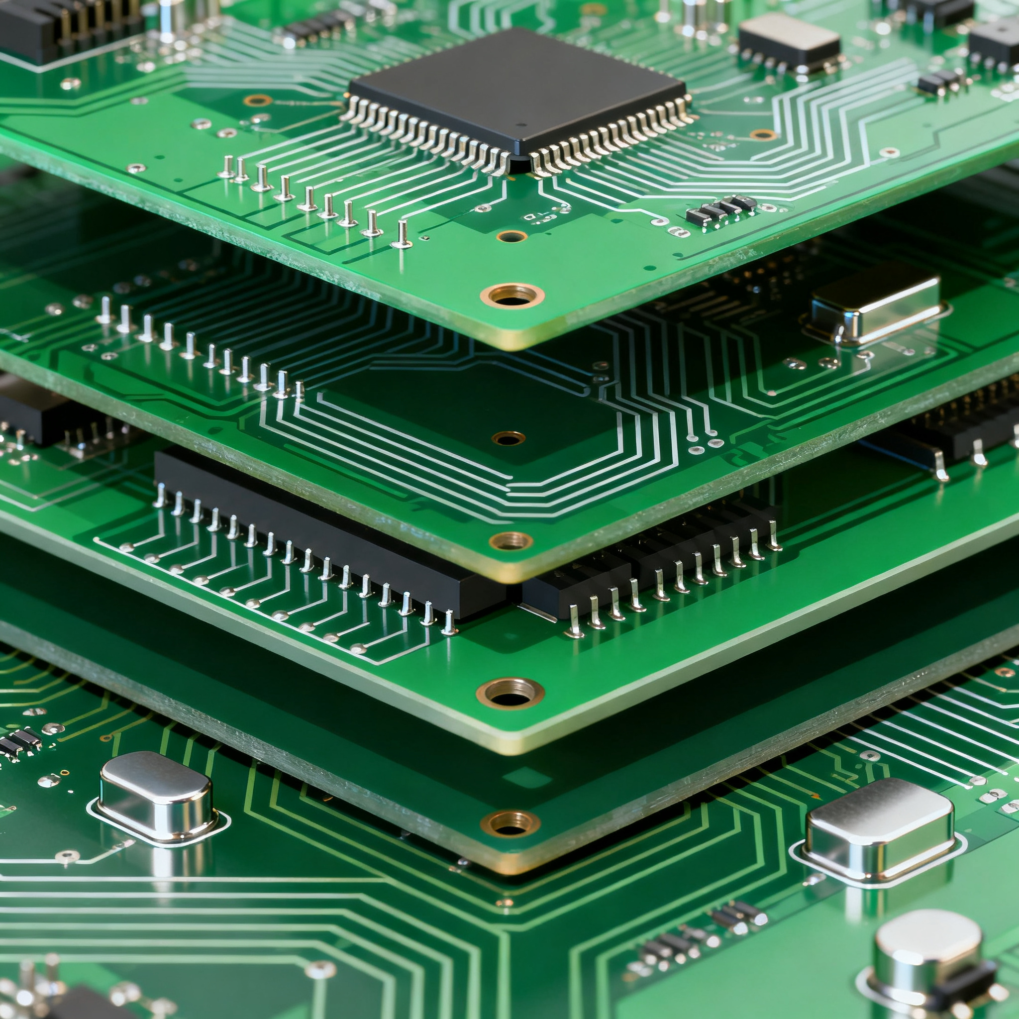
PCB stack-up refers to the arrangement of dielectric layers and copper layers in a multilayer PCB. This configuration plays a crucial role in ensuring signal integrity, power integrity, and EMI control. An 8-layer PCB stack-up typically consists of layers dedicated to signal routing, power distribution, and ground planes. The architecture of the stack-up directly impacts the electrical characteristics of the board, influencing factors such as impedance control and crosstalk. By carefully selecting materials and layer arrangements, engineers can optimize the board for specific applications, ensuring that it meets performance requirements while maintaining manufacturability and cost-effectiveness.
Detailed Specifications
Understanding the key specifications of an 8-layer PCB is fundamental for achieving optimal performance. These specifications include parameters such as dielectric constant, layer thickness, and copper weight, which influence the electrical and thermal behavior of the board. The following table outlines the main parameters and ratings critical for designing an efficient 8-layer PCB configuration.
| Parameter | Specification | Importance |
|---|---|---|
| Dielectric Constant (Er) | 4.5 | Influences signal speed and impedance |
| Layer Thickness | 0.18 mm | Affects impedance and signal integrity |
| Copper Weight | 1 oz | Determines current carrying capacity |
| Thermal Conductivity | 0.3 W/mK | Impacts heat dissipation |
| Impedance Control | ±10% | Ensures signal integrity |
| Maximum Current | 3 A | Limits power handling |
| Operating Temperature | -40°C to 85°C | Defines environmental suitability |
| Peel Strength | 1.5 N/mm | Ensures mechanical reliability |
| Surface Finish | ENIG | Prevents oxidation and improves solderability |
| Glass Transition Temperature (Tg) | 150°C | Defines thermal stability |
Key Takeaways from the Specifications
The specifications outlined in the table highlight the critical parameters that must be considered when designing an 8-layer PCB. The dielectric constant and layer thickness are pivotal in controlling impedance and ensuring signal integrity, which are crucial for high-speed applications. Copper weight directly affects the board's ability to handle current, influencing both thermal management and electrical performance. The operating temperature range and glass transition temperature (Tg) provide insights into the environmental conditions under which the PCB can reliably function. By understanding these specifications, engineers can make informed decisions that align with the performance and reliability goals of their projects.
Performance Metrics
Performance metrics for an 8-layer PCB configuration go beyond basic specifications, focusing on the electrical and thermal characteristics that determine the board's real-world performance. These metrics provide insights into how the board will behave under different operating conditions, influencing design choices and application suitability.
| Metric | Value | Significance |
|---|---|---|
| Signal Loss | 0.02 dB/inch | Impacts data transmission efficiency |
| Crosstalk | 30 dB | Affects signal integrity |
| Thermal Resistance | 15 °C/W | Determines heat dissipation |
| Power Distribution Network (PDN) Impedance | 100 mΩ | Ensures stable power delivery |
| Electromagnetic Interference (EMI) | -50 dBm | Influences compliance with standards |
| Dielectric Loss Tangent | 0.015 | Affects signal attenuation |
| Thermal Expansion Coefficient | 17 ppm/°C | Influences mechanical stability |
| Current Density | 35 A/mm² | Limits power handling capabilities |
Practical Implications
The performance metrics provided in the table serve as a guide for evaluating the real-world capabilities of an 8-layer PCB. Signal loss and crosstalk are critical for high-speed data transmission, affecting the board's ability to maintain signal integrity over long distances. Thermal resistance and thermal expansion coefficient are key factors in thermal management, ensuring that the board can effectively dissipate heat and maintain mechanical stability. Understanding these metrics allows engineers to optimize their designs for specific applications, ensuring that the PCB meets performance requirements while minimizing potential issues such as overheating or signal degradation.
Application Matrix
The application matrix provides a comprehensive overview of the various use cases and configurations for 8-layer PCBs. This matrix helps engineers and designers identify the most suitable applications for their designs, taking into account factors such as performance requirements, environmental conditions, and cost considerations.
| Use Case | Configuration | Considerations |
|---|---|---|
| High-Speed Data Processing | 4 Signal, 2 Power, 2 Ground | Focus on impedance control |
| RF Applications | 3 Signal, 3 Ground, 2 Power | Minimize crosstalk and EMI |
| Power Management | 2 Signal, 4 Power, 2 Ground | Ensure stable power delivery |
| Automotive Electronics | 3 Signal, 2 Power, 3 Ground | Consider thermal and mechanical stability |
| Consumer Electronics | 4 Signal, 2 Ground, 2 Power | Balance performance and cost |
| Telecommunications | 2 Signal, 3 Ground, 3 Power | Optimize for signal integrity |
| Medical Devices | 3 Signal, 2 Power, 3 Ground | Ensure reliability and safety |
Application Guidelines
The application matrix illustrates the diverse range of configurations and use cases for 8-layer PCBs. For high-speed data processing, configurations with multiple signal layers and strict impedance control are essential to maintain data integrity. RF applications benefit from a focus on minimizing crosstalk and EMI, which can be achieved through careful layer arrangement and grounding strategies. Power management applications require configurations that emphasize stable power delivery, often involving multiple power layers. By consulting the matrix, engineers can tailor their designs to meet the specific demands of their applications, ensuring optimal performance and reliability.
Design Considerations
Designing an 8-layer PCB involves a myriad of considerations that extend beyond basic specifications and performance metrics. Engineers must account for factors such as signal integrity, power distribution, thermal management, and manufacturability. Signal integrity is paramount in high-speed applications, necessitating careful impedance control and crosstalk minimization. Power distribution networks (PDNs) must be designed to ensure stable voltage levels across the board, often requiring dedicated power and ground planes. Thermal management is crucial for preventing overheating and maintaining reliability, which can be achieved through appropriate layer arrangements and material selection. Additionally, manufacturability considerations, such as layer alignment and via placement, play a vital role in ensuring that the PCB can be produced efficiently and cost-effectively.
Step-by-Step Implementation
Implementing an optimized 8-layer PCB stack-up requires a systematic approach to design and manufacturing. The following step-by-step guide outlines the key stages involved in developing a high-performance PCB:
- Define Requirements: Begin by identifying the specific performance requirements and constraints of your application, including signal integrity, power handling, and environmental conditions.
- Select Materials: Choose appropriate dielectric materials and copper weights based on the electrical and thermal characteristics needed for your design.
- Design Stack-Up: Develop an initial stack-up configuration, considering the arrangement of signal, power, and ground layers to optimize impedance and minimize crosstalk.
- Simulate Performance: Use simulation tools to evaluate the electrical and thermal performance of the stack-up, making adjustments as necessary to meet design goals.
- Optimize Layout: Refine the PCB layout to ensure efficient routing, proper via placement, and adherence to design rules and standards.
- Prototype and Test: Manufacture a prototype of the PCB and conduct thorough testing to validate performance against specifications and identify any potential issues.
- Iterate and Refine: Based on test results, make necessary adjustments to the design and manufacturing process to optimize performance and reliability.
- Finalize Design: Once the design meets all performance and manufacturability criteria, finalize the design for mass production, ensuring compliance with relevant standards and regulations.
Common Issues & Solutions
Despite careful planning and design, engineers may encounter common issues during the development of an 8-layer PCB. The following are some typical problems and their solutions:
- Signal Integrity Issues: Use impedance-controlled traces and proper termination techniques to minimize signal reflections and maintain integrity.
- Crosstalk: Increase spacing between signal traces and use ground planes to shield sensitive signals from interference.
- Thermal Management Challenges: Implement thermal vias and use materials with high thermal conductivity to enhance heat dissipation.
- Power Distribution Problems: Design robust PDNs with adequate decoupling capacitors to ensure stable voltage levels across the board.
- Manufacturing Defects: Conduct thorough design rule checks (DRC) and work closely with manufacturers to ensure that the design is producible within their capabilities.
- EMI Compliance: Implement proper grounding and shielding techniques to minimize emissions and meet regulatory standards.
Applications & Use Cases
8-layer PCBs find applications across a wide range of industries, each with unique performance requirements and design challenges. In telecommunications, these boards are used to support high-speed data transmission and signal integrity. Automotive electronics benefit from the thermal management capabilities and mechanical stability provided by optimized stack-ups. In the medical field, 8-layer PCBs are employed in devices that require high reliability and safety standards. Consumer electronics utilize these PCBs to balance performance and cost, delivering feature-rich products in compact form factors. By tailoring the stack-up configuration to the specific needs of each application, engineers can achieve optimal performance and reliability.
Selection & Sourcing Guide
When selecting components and materials for an 8-layer PCB, engineers should consider factors such as performance specifications, cost, and availability. It is essential to source components from reputable suppliers who provide detailed datasheets and technical support. For more information on sourcing electronic components, visit IC Online, a comprehensive resource for electronic components and suppliers.
FAQ
The following frequently asked questions address common concerns and considerations related to 8-layer PCB design and optimization:
- What is the advantage of using an 8-layer PCB? An 8-layer PCB offers improved signal integrity, power distribution, and thermal management compared to lower-layer configurations, making it suitable for complex and high-performance applications.
- How do I ensure impedance control in my PCB design? Use controlled impedance traces and maintain consistent trace geometry and spacing to achieve the desired impedance levels.
- What materials are recommended for high-frequency applications? Low-loss dielectric materials with a low dielectric constant and loss tangent are ideal for high-frequency applications, as they minimize signal attenuation.
- How can I minimize EMI in my PCB design? Implement proper grounding, shielding, and layer arrangement techniques to reduce electromagnetic emissions and ensure compliance with standards.
- What are the key considerations for thermal management? Use materials with high thermal conductivity, implement thermal vias, and ensure adequate airflow to effectively dissipate heat.
- How do I select the right surface finish for my PCB? Consider factors such as solderability, oxidation resistance, and environmental conditions when choosing a surface finish, with common options including ENIG and HASL.
- What is the role of a power distribution network (PDN)? The PDN ensures stable power delivery across the PCB, minimizing voltage fluctuations and supporting reliable operation of components.
- How can I improve the manufacturability of my PCB design? Conduct thorough design rule checks, optimize layer alignment, and collaborate with manufacturers to ensure the design is producible within their capabilities.
- What tools are available for simulating PCB performance? Simulation tools such as Ansys HFSS, Cadence Allegro, and Altium Designer provide comprehensive capabilities for evaluating electrical and thermal performance.
- How do I balance performance and cost in my PCB design? Prioritize critical performance parameters and explore cost-effective material and manufacturing options to achieve the desired balance.
Conclusion
Optimizing the stack-up of an 8-layer PCB is a complex but rewarding endeavor, offering significant performance improvements in terms of signal integrity, power distribution, and thermal management. By understanding the key specifications, performance metrics, and application guidelines, engineers can design PCBs that meet the demanding requirements of modern electronic devices. With careful planning, simulation, and collaboration with manufacturers, the full potential of 8-layer PCBs can be realized, driving innovation and reliability across a wide range of applications.