Maximize Efficiency: Top PCB Design Software Tools for 4-Layer Boards
Introduction In the rapidly evolving field of electronics, efficiency in printed circuit board (PCB) design is paramount. As devices become more compact and powerful, the need for sophisticated design...
Introduction
In the rapidly evolving field of electronics, efficiency in printed circuit board (PCB) design is paramount. As devices become more compact and powerful, the need for sophisticated design tools that can handle complex multilayer boards, such as 4-layer PCBs, has become crucial. These tools are not only vital for optimizing layout design but also for ensuring that electrical performance meets the stringent demands of modern applications. By leveraging advanced PCB design software, engineers can enhance productivity, reduce errors, and accelerate time-to-market, ensuring competitive advantage in a fast-paced industry.
Technical Overview
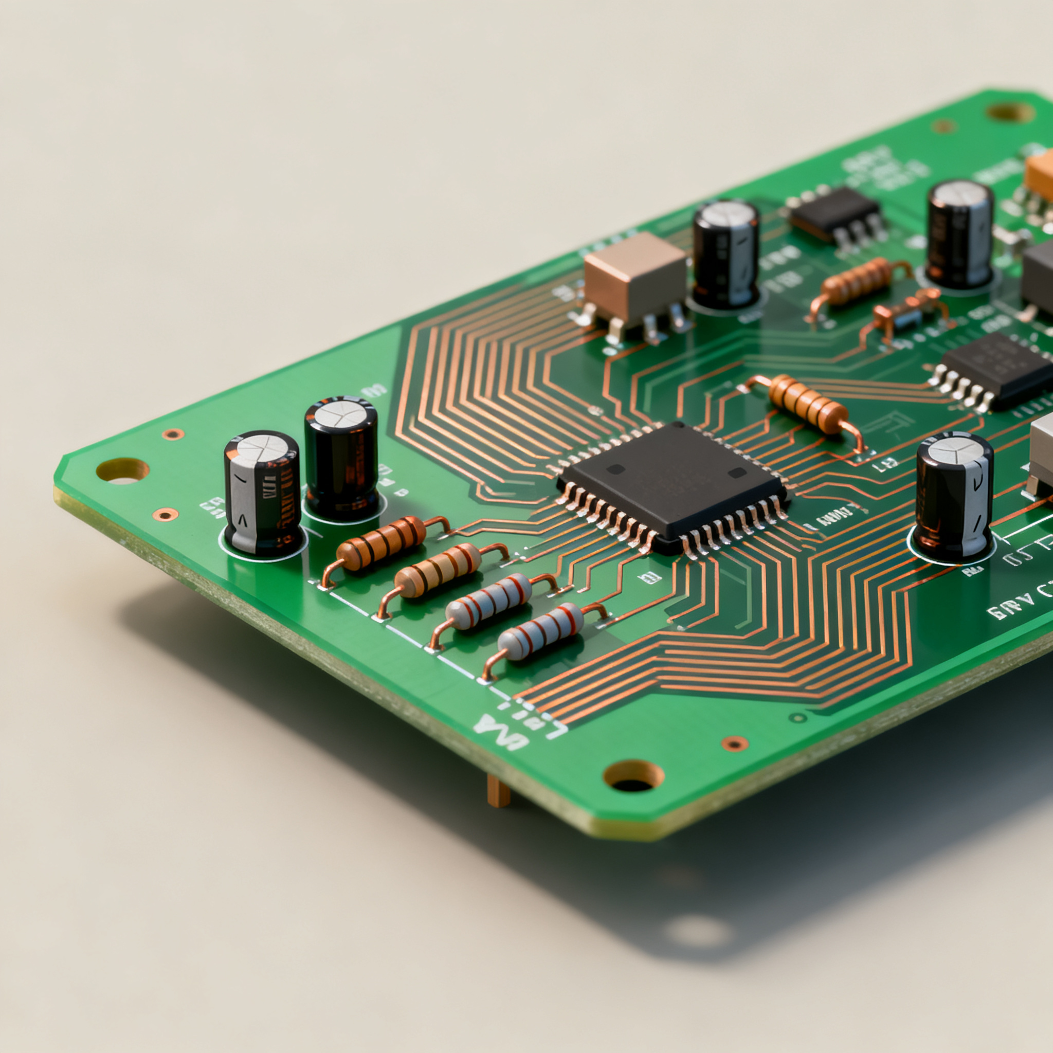
PCB design is a meticulous process that involves creating a blueprint for electronic circuits. A 4-layer PCB typically consists of two outer layers and two inner layers, allowing for more complex and densely packed circuits compared to single or double-layer boards. The architecture of a 4-layer board includes signal layers, a ground plane, and a power plane, which help in minimizing electromagnetic interference (EMI) and improving signal integrity.
The principles of PCB design revolve around efficient signal routing, minimizing trace lengths, and ensuring adequate power distribution. Advanced design software tools come equipped with features such as auto-routing, design rule checks, and simulation capabilities, which are essential for optimizing the performance of 4-layer boards. Understanding the core concepts of PCB design, such as stack-up configuration and impedance control, is crucial for maximizing the efficiency of these tools.
Detailed Specifications
When selecting components for a 4-layer PCB, understanding the core specifications is vital. Key parameters such as CPU speed, memory capacity, peripheral interfaces, power requirements, and packaging options can significantly impact the performance and functionality of the final product. The following table provides an overview of important specifications to consider during the design phase.
| Specification | Details | Importance |
|---|---|---|
| CPU Speed | 1.2 GHz | Determines processing capability |
| Memory | 512 MB DDR3 | Affects data handling capacity |
| Peripherals | USB, Ethernet, SPI | Enables connectivity and expansion |
| Power Supply | 3.3V, 5V | Influences power management |
| Package Type | LQFP, BGA | Impacts assembly and thermal performance |
| Operating Temperature | -40°C to 85°C | Defines environmental suitability |
| Storage Temperature | -55°C to 125°C | Ensures durability |
| Dimensions | 100mm x 100mm | Affects form factor compatibility |
| Weight | 50 grams | Influences mechanical design |
| Compliance | RoHS, CE | Ensures regulatory adherence |
Key Takeaways from the Specifications
The specifications outlined in the table above highlight critical factors that influence the design and functionality of a 4-layer PCB. CPU speed and memory are pivotal in determining the processing power and data handling capacity of the board. Peripheral interfaces such as USB and Ethernet enhance connectivity options, making the board suitable for a wide range of applications. Power supply specifications are crucial for effective power management, while package type impacts the assembly process and thermal performance. Understanding these specifications allows engineers to make informed decisions during the component selection process, ultimately leading to more efficient and reliable PCB designs.
| Parameter | Value | Significance |
|---|---|---|
| Operating Voltage | 3.3V | Standard for low-power applications |
| Max Current | 500mA | Defines current handling capability |
| Input Logic Level | 0.8V (Low), 2.0V (High) | Ensures compatibility with logic families |
| Output Logic Level | 0.4V (Low), 2.4V (High) | Affects signal integrity |
| Propagation Delay | 5ns | Impacts timing accuracy |
| Rise/Fall Time | 2ns | Critical for high-speed applications |
| ESD Protection | ±2kV | Ensures robustness against electrostatic discharge |
| Power Dissipation | 1W | Influences thermal management |
| Leakage Current | 10µA | Affects power efficiency |
| Noise Margin | 0.4V | Ensures reliable signal transmission |
Practical Implications
The electrical characteristics table provides insights into the operational parameters of components used in 4-layer PCB designs. Operating voltage and current ratings are crucial for ensuring that the board can handle the required power levels without overheating. Input and output logic levels are essential for maintaining signal compatibility across different components. Parameters such as propagation delay and rise/fall time are particularly important for high-speed applications, where timing accuracy is critical. Understanding these electrical characteristics helps engineers optimize the performance and reliability of their PCB designs, especially in demanding environments.
| Application | Configuration | Benefits |
|---|---|---|
| Consumer Electronics | High-speed data processing | Enhanced user experience |
| Industrial Automation | Robust power management | Improved reliability and uptime |
| Automotive Systems | EMI shielding | Increased safety and compliance |
| Medical Devices | Compact form factor | Portability and ease of use |
| Telecommunications | High-frequency signal handling | Better connectivity and speed |
| Aerospace Applications | Temperature resilience | Operational stability in extreme conditions |
Application Guidelines
The application comparison table highlights various use cases for 4-layer PCBs, each with specific configurations and benefits. For instance, consumer electronics benefit from high-speed data processing capabilities, enhancing the overall user experience. In industrial automation, robust power management ensures reliability and reduces downtime. EMI shielding is crucial in automotive systems to enhance safety and compliance with regulatory standards. Understanding these applications and configurations helps engineers tailor their PCB designs to meet the specific needs of different industries, ensuring optimal performance and efficiency.
Design Considerations
Designing a 4-layer PCB involves several critical considerations to ensure optimal performance and manufacturability. One of the primary factors is the stack-up configuration, which determines the arrangement of signal, power, and ground layers. Proper stack-up design minimizes signal interference and enhances EMI shielding, crucial for high-speed and high-frequency applications.
Another important consideration is trace routing. Efficient routing reduces trace lengths and minimizes cross-talk, which is essential for maintaining signal integrity. Engineers must also consider the placement of components, ensuring that high-frequency components are placed close to each other to reduce latency and enhance performance.
Thermal management is another key aspect of PCB design. Adequate heat dissipation is necessary to prevent overheating and ensure the longevity of components. This can be achieved through the use of thermal vias, heat sinks, and appropriate board materials.
Compliance with industry standards, such as IPC-A-610 and IPC-2221, is also critical. These standards provide guidelines for PCB design, assembly, and quality inspection, ensuring that the final product meets the required quality and reliability benchmarks. By considering these design aspects, engineers can create efficient, reliable, and cost-effective 4-layer PCB designs.
Step-by-Step Implementation
- Define Requirements: Identify the specific requirements of the PCB, including functionality, size, and environmental conditions.
- Select Components: Choose components based on the detailed specifications and electrical characteristics outlined earlier.
- Design Schematic: Create a schematic diagram using PCB design software, ensuring that all connections and components are accurately represented.
- Design Layout: Develop the PCB layout, considering factors such as trace routing, component placement, and layer stack-up.
- Run Design Rule Checks: Use design rule checking (DRC) tools to identify and correct any design violations or errors.
- Simulate Design: Perform simulations to verify the electrical performance and signal integrity of the PCB design.
- Generate Gerber Files: Create Gerber files, which are essential for the manufacturing process, detailing the PCB layout and layer information.
- Prototype and Test: Manufacture a prototype PCB and conduct thorough testing to validate the design and functionality.
Common Issues & Solutions
- Signal Integrity Issues: Use controlled impedance traces and proper termination techniques to reduce reflections and maintain signal quality.
- Thermal Management Problems: Implement thermal vias and heat sinks to improve heat dissipation and prevent component damage.
- EMI Interference: Utilize ground planes and shielding techniques to minimize electromagnetic interference.
- Power Distribution Challenges: Design power planes with adequate width and use decoupling capacitors to ensure stable power distribution.
- Component Placement Errors: Follow placement guidelines to minimize trace lengths and reduce cross-talk between components.
- Manufacturing Defects: Adhere to IPC standards and perform thorough inspections to identify and rectify manufacturing defects.
Applications & Use Cases
4-layer PCBs are widely used across various industries due to their enhanced capabilities and compact design. In consumer electronics, they enable high-speed data processing and connectivity, crucial for devices such as smartphones and tablets. Industrial automation systems benefit from their robust power management and reliability, essential for maintaining operational efficiency. In the automotive sector, 4-layer PCBs provide EMI shielding and compliance with safety standards, vital for advanced driver-assistance systems (ADAS) and infotainment systems.
Medical devices, such as portable diagnostic equipment, leverage the compact form factor of 4-layer PCBs to offer portability and ease of use. Telecommunications infrastructure relies on their ability to handle high-frequency signals, ensuring better connectivity and speed. In aerospace applications, the temperature resilience of 4-layer PCBs ensures operational stability in extreme conditions, making them ideal for avionics and satellite systems.
Selection & Sourcing Guide
When selecting components for a 4-layer PCB, it is essential to consider the specifications and electrical characteristics outlined earlier. Reputable sources such as IC Online offer a wide range of components, ensuring compliance with industry standards and quality benchmarks. Engineers should evaluate suppliers based on factors such as pricing, lead times, and customer support to ensure a smooth sourcing process.
FAQ
- What is a 4-layer PCB? A 4-layer PCB consists of four layers, typically two outer signal layers and two inner layers for power and ground planes.
- Why use a 4-layer PCB? 4-layer PCBs offer improved signal integrity, EMI shielding, and power distribution, making them suitable for complex applications.
- What software tools are recommended for 4-layer PCB design? Popular tools include Altium Designer, Eagle, and KiCad, which offer advanced features for multilayer designs.
- How does stack-up configuration affect PCB performance? Proper stack-up minimizes signal interference and enhances EMI shielding, crucial for high-speed applications.
- What are the key considerations for component placement? Components should be placed to minimize trace lengths and reduce cross-talk, ensuring optimal performance.
- How can I ensure compliance with IPC standards? Adhering to design guidelines and performing thorough inspections ensures compliance with IPC-A-610 and IPC-2221 standards.
- What are the common issues in 4-layer PCB design? Issues include signal integrity problems, thermal management challenges, and EMI interference, which can be mitigated with proper design techniques.
- How do I select components for a 4-layer PCB? Consider specifications such as CPU speed, memory, and electrical characteristics to ensure compatibility and performance.
- What is the role of power planes in a 4-layer PCB? Power planes distribute power evenly across the board, ensuring stable operation and reducing voltage drop.
- How does trace routing impact PCB performance? Efficient routing minimizes trace lengths and reduces cross-talk, maintaining signal integrity and reliability.
Conclusion
Maximizing efficiency in 4-layer PCB design is crucial for meeting the demands of modern electronic applications. By leveraging advanced design tools and adhering to industry standards, engineers can create reliable and high-performance PCBs. Understanding the detailed specifications and electrical characteristics of components is essential for optimizing design and ensuring compatibility with various applications. By following best practices and addressing common design challenges, engineers can deliver innovative solutions that meet the needs of diverse industries.