Maximize Efficiency: Choosing the Right PCB Assembly Service for Your 4-Layer Design
Introduction In the rapidly evolving world of electronics, choosing the right PCB assembly service is crucial for maximizing efficiency, especially for complex designs like a 4-layer PCB. As devices b...
Introduction
In the rapidly evolving world of electronics, choosing the right PCB assembly service is crucial for maximizing efficiency, especially for complex designs like a 4-layer PCB. As devices become more sophisticated, the demand for compact, efficient, and reliable PCBs has surged. A well-chosen PCB assembly service can significantly impact the performance, cost, and time-to-market of your product. This article delves into the critical components, specifications, and services you need to consider while selecting a PCB assembly service for your 4-layer design.
Technical Overview
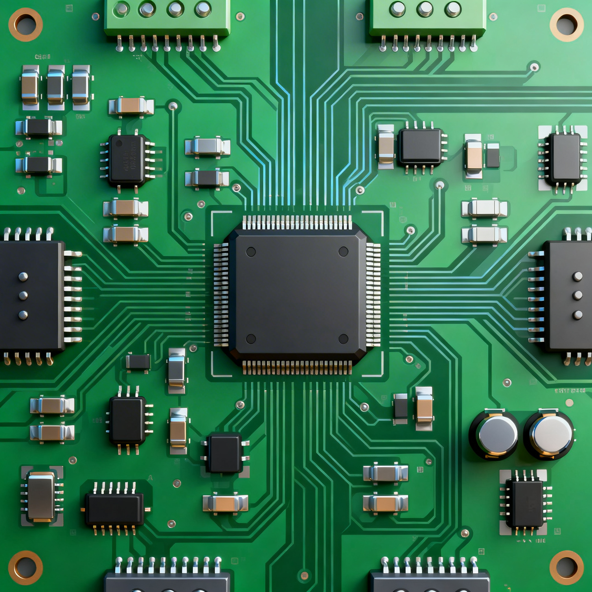
4-layer PCBs are commonly used in applications requiring complex circuitry and high performance. They consist of four layers of copper separated by insulating material, allowing for increased circuit density and improved signal integrity. The architecture of a 4-layer PCB typically includes a ground plane, a power plane, and two signal layers. This configuration helps in minimizing electromagnetic interference and improving thermal management. Key principles in designing a 4-layer PCB include careful layer stack-up planning, impedance control, and thermal considerations. By understanding these core concepts, engineers can leverage the full potential of 4-layer PCBs in their applications.
Detailed Specifications
When selecting components for your 4-layer PCB design, understanding the core specifications is crucial. These specifications help in determining the compatibility and performance of the components in your design. Important specifications include CPU speed, memory capacity, peripheral interfaces, power requirements, and package type. These factors influence the overall efficiency and functionality of the PCB.
| Specification | Details | Importance |
|---|---|---|
| CPU Speed | 1.2 GHz | Determines processing power |
| Memory | 4GB DDR4 | Influences multitasking capability |
| Peripherals | USB, HDMI, Ethernet | Connectivity options |
| Power | 12V, 3A | Operational power requirement |
| Package | BGA | Space-saving and thermal efficiency |
| Operating Temperature | -40°C to 85°C | Ensures reliability in various environments |
| Storage | 64GB eMMC | Data storage capacity |
| Dimensions | 100mm x 100mm | Size for design compatibility |
| Weight | 50g | Influences portability |
| Compliance | RoHS, CE | Meets safety and environmental standards |
Key Takeaways from the Specifications
Understanding the core specifications of your PCB components is vital for ensuring optimal performance and compatibility with your design requirements. CPU speed and memory are crucial for determining the processing power and multitasking capabilities of your device. Peripherals such as USB and HDMI are important for connectivity and user interaction. Power specifications, including voltage and current requirements, are essential for ensuring that your PCB operates efficiently without overheating. Additionally, package type and compliance with standards like RoHS and CE ensure that your design is both compact and meets necessary safety standards. These specifications serve as a foundation for making informed decisions during the design and manufacturing process.
| Electrical Characteristic | Value | Significance |
|---|---|---|
| Operating Voltage | 3.3V | Standard voltage level for logic circuits |
| Current Consumption | 500mA | Determines power efficiency |
| Signal Rise Time | 2ns | Affects signal integrity |
| Input Impedance | 50Ω | Ensures minimal signal reflection |
| Output Drive Strength | 10mA | Ability to drive loads |
| Clock Frequency | 100MHz | Determines data processing speed |
| Leakage Current | 5µA | Impacts battery life |
| ESD Protection | ±15kV | Prevents electrostatic damage |
| Thermal Resistance | 35°C/W | Influences thermal management |
| Noise Margin | 1V | Ensures reliable signal transmission |
| I/O Voltage Levels | 1.8V to 5V | Compatibility with various components |
| Power Dissipation | 1.5W | Limits thermal output |
Practical Implications
The electrical characteristics of your PCB components have a direct impact on the performance and reliability of your design. Operating voltage and current consumption are crucial for determining the power efficiency and operational stability of the PCB. Signal rise time and input impedance are important for maintaining signal integrity and preventing data errors. Output drive strength and clock frequency influence the ability of the PCB to process and transmit data effectively. Additionally, considerations such as ESD protection and thermal resistance are essential for ensuring that the PCB can withstand environmental stresses and operate reliably under various conditions. By understanding these electrical characteristics, engineers can design PCBs that are both efficient and robust.
| Application | Configuration | Benefits |
|---|---|---|
| Consumer Electronics | Standard 4-layer | Cost-effective and compact |
| Automotive Systems | High durability | Withstands harsh environments |
| Industrial Controls | Enhanced thermal management | Reliable in high-temperature settings |
| Telecommunications | High-speed data processing | Efficient data transmission |
| Medical Devices | Miniaturized design | Portable and efficient |
| Aerospace Applications | High reliability | Operates in extreme conditions |
| IoT Devices | Low power consumption | Extended battery life |
Application Guidelines
When selecting a PCB assembly service for your 4-layer design, it is important to consider the specific applications and configurations of your product. For consumer electronics, a standard 4-layer configuration offers a cost-effective and compact solution. In automotive and aerospace applications, high durability and reliability are essential to withstand harsh environments. Industrial controls benefit from enhanced thermal management, making them reliable in high-temperature settings. For telecommunications, high-speed data processing is crucial for efficient data transmission. Medical devices require miniaturized designs for portability, while IoT devices benefit from low power consumption to extend battery life. By aligning your PCB design with the specific needs of your application, you can ensure optimal performance and reliability.
Design Considerations
Designing a 4-layer PCB requires careful consideration of several factors to ensure optimal performance and reliability. One of the primary design considerations is the layer stack-up, which affects signal integrity and thermal management. A typical stack-up might include a ground plane, power plane, and two signal layers. Properly planning the stack-up can minimize electromagnetic interference and improve heat dissipation. Impedance control is another critical aspect, especially in high-speed applications, where maintaining consistent impedance is crucial for signal integrity. Designers must also consider the placement and routing of components to minimize trace lengths and avoid crosstalk. Thermal management is vital, especially in high-power applications, where heat dissipation can affect performance and reliability. Utilizing thermal vias and heat sinks can help manage heat effectively. Additionally, ensuring compliance with industry standards such as IPC-A-610 and IPC-2221 is crucial for quality and reliability. By addressing these design considerations, engineers can create efficient and reliable 4-layer PCBs that meet the demands of their applications.
Step-by-Step Implementation
Implementing a 4-layer PCB design involves several detailed steps to ensure successful assembly and operation. Here is a step-by-step guide:
- Define the Requirements: Start by clearly defining the requirements of your PCB, including size, power, and performance specifications.
- Design the Schematic: Use PCB design software to create the schematic, ensuring all components and connections are accurately represented.
- Create the Layer Stack-Up: Plan the layer stack-up, considering signal integrity, power distribution, and thermal management.
- Component Placement: Place components strategically to minimize trace lengths and avoid crosstalk while ensuring accessibility for testing and maintenance.
- Routing: Route the traces, focusing on maintaining consistent impedance and minimizing electromagnetic interference.
- Thermal Management: Incorporate thermal vias and heat sinks as needed to manage heat dissipation effectively.
- Design Rule Check (DRC): Perform a DRC to ensure the design adheres to industry standards and manufacturing capabilities.
- Prototype and Testing: Manufacture a prototype and conduct thorough testing to identify and resolve any issues before final production.
By following these steps, engineers can efficiently implement a 4-layer PCB design that meets the desired specifications and performance criteria.
Common Issues & Solutions
During the design and assembly of a 4-layer PCB, several common issues may arise. Here are some real problems and their solutions:
- Signal Integrity Issues: Poor signal integrity can result from improper routing or impedance mismatches. Solution: Ensure proper impedance control and minimize trace lengths.
- Thermal Management Challenges: Excessive heat can affect performance and reliability. Solution: Use thermal vias, heat sinks, and appropriate layer stack-up for better heat dissipation.
- Electromagnetic Interference (EMI): EMI can disrupt circuit performance. Solution: Utilize proper grounding techniques and shielding to minimize interference.
- Manufacturing Defects: Defects such as solder bridges can occur during assembly. Solution: Follow IPC standards and conduct thorough inspection and testing.
- Component Placement Errors: Incorrect placement can cause connectivity issues. Solution: Use design software with placement verification features.
- Power Distribution Problems: Inadequate power distribution can lead to voltage drops. Solution: Design a robust power plane and use decoupling capacitors effectively.
By addressing these common issues proactively, engineers can enhance the reliability and performance of their 4-layer PCB designs.
Applications & Use Cases
4-layer PCBs are widely used in various applications due to their ability to handle complex circuitry and high performance. In consumer electronics, they provide a compact and cost-effective solution for smartphones, tablets, and wearable devices. In the automotive industry, 4-layer PCBs are used in advanced driver-assistance systems (ADAS) and infotainment systems, where durability and reliability are critical. Industrial controls utilize 4-layer PCBs for automation and process control, benefiting from enhanced thermal management. Telecommunications equipment relies on 4-layer PCBs for high-speed data processing and efficient signal transmission. Medical devices, such as portable diagnostic tools, require miniaturized designs that 4-layer PCBs can accommodate. In aerospace applications, the high reliability and ability to operate in extreme conditions make 4-layer PCBs an ideal choice. By understanding the diverse applications and use cases, engineers can leverage the advantages of 4-layer PCBs in their designs.
Selection & Sourcing Guide
When selecting and sourcing components for your 4-layer PCB design, it is important to consider factors such as performance, reliability, and cost. Start by reviewing datasheets and specifications to ensure compatibility with your design requirements. Utilize online resources such as IC Online to find a wide range of components from reputable manufacturers. Consider working with PCB assembly services like PCBWay and Nova PCBA that offer flexible manufacturing capabilities and quick turnaround times. By carefully selecting and sourcing components, you can enhance the performance and reliability of your 4-layer PCB design while keeping costs under control.
FAQ
Here are some frequently asked questions regarding 4-layer PCB design and assembly:
- What are the advantages of a 4-layer PCB? 4-layer PCBs offer improved signal integrity, enhanced thermal management, and increased circuit density compared to 2-layer PCBs.
- How do I choose the right PCB assembly service? Consider factors such as manufacturing capabilities, turnaround time, and adherence to industry standards when selecting a PCB assembly service.
- What is the importance of layer stack-up in a 4-layer PCB? Proper layer stack-up is crucial for minimizing electromagnetic interference and ensuring efficient power distribution.
- How can I ensure signal integrity in my PCB design? Maintain consistent impedance, minimize trace lengths, and use proper grounding techniques to ensure signal integrity.
- What are the common causes of EMI in PCB designs? EMI can be caused by improper grounding, inadequate shielding, and poor component placement.
- How do I manage thermal issues in a 4-layer PCB? Use thermal vias, heat sinks, and appropriate layer stack-up to manage heat dissipation effectively.
- What standards should my PCB design comply with? Ensure compliance with IPC standards such as IPC-A-610 and IPC-2221 for quality and reliability.
- How do I reduce power consumption in my PCB design? Use low-power components and optimize power distribution networks to reduce power consumption.
- What are the key considerations for component placement? Minimize trace lengths, avoid crosstalk, and ensure accessibility for testing and maintenance.
- How can I improve the reliability of my PCB design? Conduct thorough testing, adhere to industry standards, and address potential issues during the design phase to improve reliability.
Conclusion
Choosing the right PCB assembly service for your 4-layer design is essential for maximizing efficiency and ensuring optimal performance. By understanding the core specifications, electrical characteristics, and application guidelines, engineers can make informed decisions that align with their design requirements. Careful consideration of design factors and proactive management of common issues can enhance the reliability and functionality of 4-layer PCBs. With the right approach, engineers can leverage the advantages of 4-layer PCBs to create innovative and efficient electronic products.