Mastering PCB Manufacturing and Assembly: A Step-by-Step Guide to Optimizing Your Production Process
Mastering PCB Manufacturing and Assembly: A Step-by-Step Guide to Optimizing Your Production Process Introduction In the rapidly advancing world of electronics, Printed Circuit Boards (PCBs) form the ...
Introduction
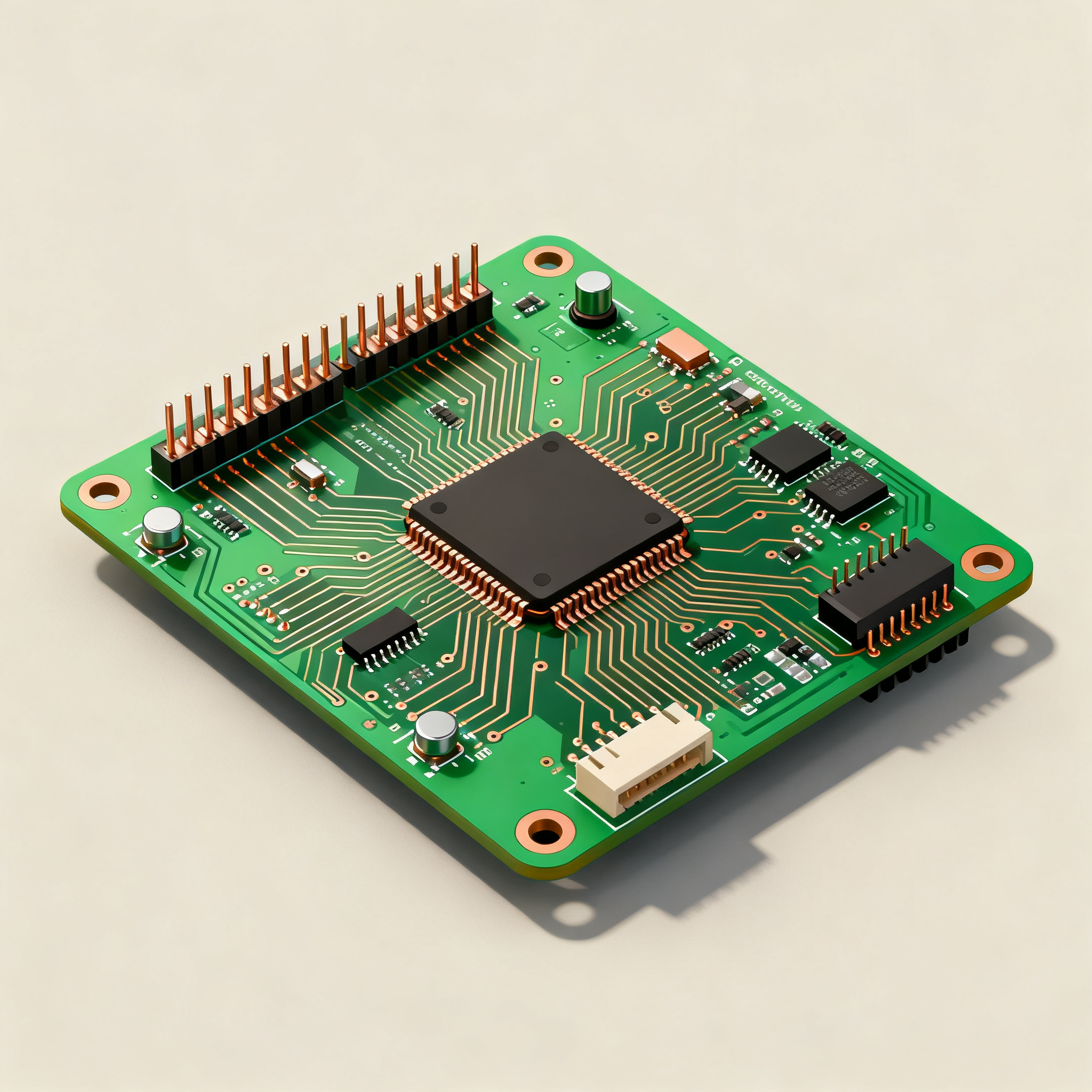
In the rapidly advancing world of electronics, Printed Circuit Boards (PCBs) form the backbone of virtually all electronic devices. Mastering the manufacturing and assembly of PCBs is crucial for ensuring the reliability and performance of electronic products. This article provides a comprehensive guide to optimizing your PCB production process, focusing on layout rules, stackup design, signal integrity, and manufacturing considerations.
Technical Overview
PCBs are essential for connecting electrical components in a structured manner, and their design requires adherence to specific rules and standards. The architecture of a PCB involves multiple layers and materials, each contributing to the board's electrical performance and mechanical stability. Key principles include signal integrity, thermal management, and manufacturability, all of which must be considered during the design phase. By understanding these core concepts, engineers can create PCBs that meet industry standards and perform reliably in real-world applications.
Detailed Specifications
When designing a PCB, several specifications are crucial to ensure functionality and manufacturability. These include trace width, spacing, via sizes, and clearances. Adhering to these specifications helps prevent issues such as signal interference, overheating, and mechanical failure. The following table outlines common design rules that engineers should consider during the PCB design process.
| Design Parameter | Minimum Value | Recommended Value |
|---|---|---|
| Trace Width | 0.15 mm | 0.20 mm |
| Trace Spacing | 0.15 mm | 0.20 mm |
| Via Diameter | 0.30 mm | 0.50 mm |
| Annular Ring | 0.10 mm | 0.15 mm |
| Pad Clearance | 0.20 mm | 0.25 mm |
| Silkscreen Clearance | 0.10 mm | 0.13 mm |
| Hole Size | 0.25 mm | 0.30 mm |
| Solder Mask Clearance | 0.05 mm | 0.08 mm |
| Edge Clearance | 0.50 mm | 0.75 mm |
| Component Spacing | 0.50 mm | 0.75 mm |
| Board Thickness | 1.0 mm | 1.6 mm |
Key Takeaways from the Specifications
These design rules are critical for ensuring the electrical and mechanical integrity of the PCB. For instance, maintaining adequate trace width and spacing helps mitigate the risk of crosstalk and signal degradation. Proper via sizes and annular rings ensure robust connections between layers, while correct pad and solder mask clearances facilitate efficient assembly. Adhering to these specifications not only enhances performance but also simplifies manufacturing, reducing the likelihood of defects and rework.
| Layer Configuration | Number of Layers | Typical Use Case |
|---|---|---|
| Single Layer | 1 | Simple circuits, low-cost applications |
| Double Layer | 2 | Moderate complexity, consumer electronics |
| Four Layer | 4 | High-speed circuits, better signal integrity |
| Six Layer | 6 | Advanced circuits, reduced EMI |
| Eight Layer | 8 | Complex designs, enhanced power distribution |
| Ten Layer | 10 | High-density applications, RF designs |
| Twelve Layer | 12 | High-performance computing, aerospace |
Practical Implications
The choice of layer stackup significantly impacts the PCB's performance and cost. Single and double-layer boards are suitable for basic applications, while multilayer boards offer improved signal integrity and reduced electromagnetic interference (EMI). As the number of layers increases, so does the complexity and cost, making it vital to balance performance needs with budget constraints. Proper stackup design also facilitates effective power distribution and heat dissipation, crucial for high-speed and high-power applications.
| Material | Dielectric Constant (Dk) | Loss Tangent (Df) |
|---|---|---|
| FR-4 | 4.5 | 0.020 |
| Rogers 4350B | 3.66 | 0.0037 |
| Rogers 5880 | 2.20 | 0.0009 |
| Isola FR406 | 4.6 | 0.019 |
| Nelco N4000-13 | 3.7 | 0.009 |
| Arlon 85N | 3.5 | 0.004 |
| Megtron 6 | 3.5 | 0.004 |
| Panasonic R-1755 | 4.2 | 0.015 |
| DuPont Pyralux | 3.5 | 0.002 |
| Isola I-Tera MT40 | 3.45 | 0.003 |
Application Guidelines
The choice of PCB material is critical for signal integrity and thermal management. FR-4 is commonly used due to its balance of cost and performance. However, for high-frequency applications, materials like Rogers and Megtron are preferred due to their lower dielectric constants and loss tangents, which minimize signal loss. Selecting the right material involves considering the application's frequency, environmental conditions, and budget, ensuring optimal performance and reliability.
Design Considerations
Successful PCB design requires careful consideration of several factors, including electrical performance, mechanical strength, and manufacturability. Signal integrity is paramount, necessitating proper trace routing, impedance control, and termination strategies. Thermal management is also crucial, particularly for high-power applications, requiring adequate heat dissipation mechanisms such as thermal vias and heat sinks. Additionally, designers must ensure compliance with industry standards like IPC-A-610 and IPC-2221 to guarantee quality and reliability.
Step-by-Step Implementation
- Define Requirements: Begin by specifying the electrical, mechanical, and environmental requirements of the PCB, considering factors such as signal speed, power levels, and operating conditions.
- Choose Materials: Select appropriate materials based on the application's frequency, thermal requirements, and cost constraints, ensuring compatibility with manufacturing processes.
- Design the Schematic: Create a detailed schematic diagram, defining all components, connections, and electrical properties, ensuring correctness and completeness.
- Layout the PCB: Use PCB design software to layout the board, adhering to design rules for trace width, spacing, and clearances, and optimizing for signal integrity and thermal management.
- Simulate and Validate: Perform simulations to validate the design, checking for signal integrity, thermal performance, and electrical compatibility, and making necessary adjustments.
- Generate Manufacturing Files: Create Gerber files and other necessary documentation, specifying all details required for fabrication and assembly.
- Prototype and Test: Fabricate a prototype and conduct thorough testing to ensure the PCB meets all specified requirements and performs reliably under expected conditions.
- Finalize Design: After successful testing, finalize the design, making any necessary refinements before proceeding to full-scale production.
Common Issues & Solutions
- Signal Integrity Problems: Issues like crosstalk and reflections can degrade performance. Solution: Ensure proper trace routing and impedance matching.
- Thermal Management Challenges: Overheating can lead to failure. Solution: Use thermal vias, heat sinks, and adequate spacing for heat dissipation.
- Manufacturing Defects: Issues such as solder bridges and misalignment can occur. Solution: Adhere to design rules and conduct thorough inspections.
- Component Placement Errors: Incorrect placement can affect functionality. Solution: Use design software to optimize component layout and spacing.
- Material Selection Mistakes: Using the wrong material can affect performance. Solution: Carefully evaluate material properties and application requirements.
- Compliance Issues: Non-compliance with standards can lead to rejection. Solution: Ensure designs meet relevant industry standards and regulations.
Applications & Use Cases
PCBs are used across a wide range of industries, from consumer electronics to aerospace. In consumer electronics, they are found in smartphones, computers, and home appliances, where cost and compactness are critical. In automotive applications, PCBs must withstand harsh conditions, necessitating robust materials and designs. In aerospace, high-reliability PCBs are essential for mission-critical systems, requiring advanced materials and stringent quality control.
Selection & Sourcing Guide
When selecting and sourcing PCBs, consider factors such as supplier capabilities, material options, and compliance with industry standards. For sourcing components, IC Online offers a wide range of electronic components, providing a convenient platform for finding and purchasing the necessary parts for your PCB projects.
FAQ
- What is the importance of trace width in PCB design? Trace width affects the current-carrying capacity and signal integrity, requiring careful consideration to prevent overheating and signal loss.
- How do I choose the right PCB material? Consider factors like frequency, thermal conditions, and cost. High-frequency applications benefit from materials with low dielectric constants and loss tangents.
- What are the benefits of a multilayer PCB? Multilayer PCBs offer improved signal integrity, reduced EMI, and better power distribution, suitable for complex and high-speed applications.
- How can I ensure compliance with IPC standards? Follow design rules and guidelines outlined in standards like IPC-A-610 and IPC-2221, and conduct thorough inspections and testing.
- What simulation tools are available for PCB design? Tools like Altium Designer, Cadence Allegro, and Mentor Graphics provide simulation capabilities for validating PCB designs.
- How do I prevent thermal issues in my PCB? Use thermal management techniques like thermal vias, heat sinks, and adequate spacing to dissipate heat effectively.
- What are common manufacturing defects in PCBs? Common defects include solder bridges, misalignment, and insufficient clearances, often due to non-compliance with design rules.
- How can I optimize PCB layout for signal integrity? Use proper trace routing, impedance control, and termination strategies to minimize signal degradation and interference.
- What factors influence PCB manufacturing costs? Costs are influenced by factors such as layer count, material choice, board size, and complexity of the design.
- How do I test a PCB prototype? Conduct electrical tests, thermal tests, and functional tests to ensure the prototype meets all specified requirements and performs reliably.
Conclusion
Mastering PCB manufacturing and assembly is essential for producing reliable and high-performance electronic products. By understanding and implementing key design rules, material properties, and manufacturing considerations, engineers can optimize their production processes. This guide provides the foundational knowledge necessary to navigate the complex world of PCB design, ensuring successful outcomes in a variety of applications.