Mastering PCB Layout Best Practices for 4-Layer Designs in 2026
Mastering PCB Layout Best Practices for 4-Layer Designs in 2026 Introduction In the rapidly evolving world of electronics, mastering PCB layout best practices for 4-layer designs has become increasing...
Introduction
In the rapidly evolving world of electronics, mastering PCB layout best practices for 4-layer designs has become increasingly critical. As we approach 2026, the demand for more compact, efficient, and reliable electronic devices continues to grow. Engineers are faced with the challenge of designing PCBs that not only meet these criteria but also adhere to stringent industry standards. This article delves into the intricacies of 4-layer PCB design, focusing on component specifications, datasheet interpretation, selection criteria, and application circuits, providing a comprehensive guide for engineers looking to excel in this field.
Technical Overview
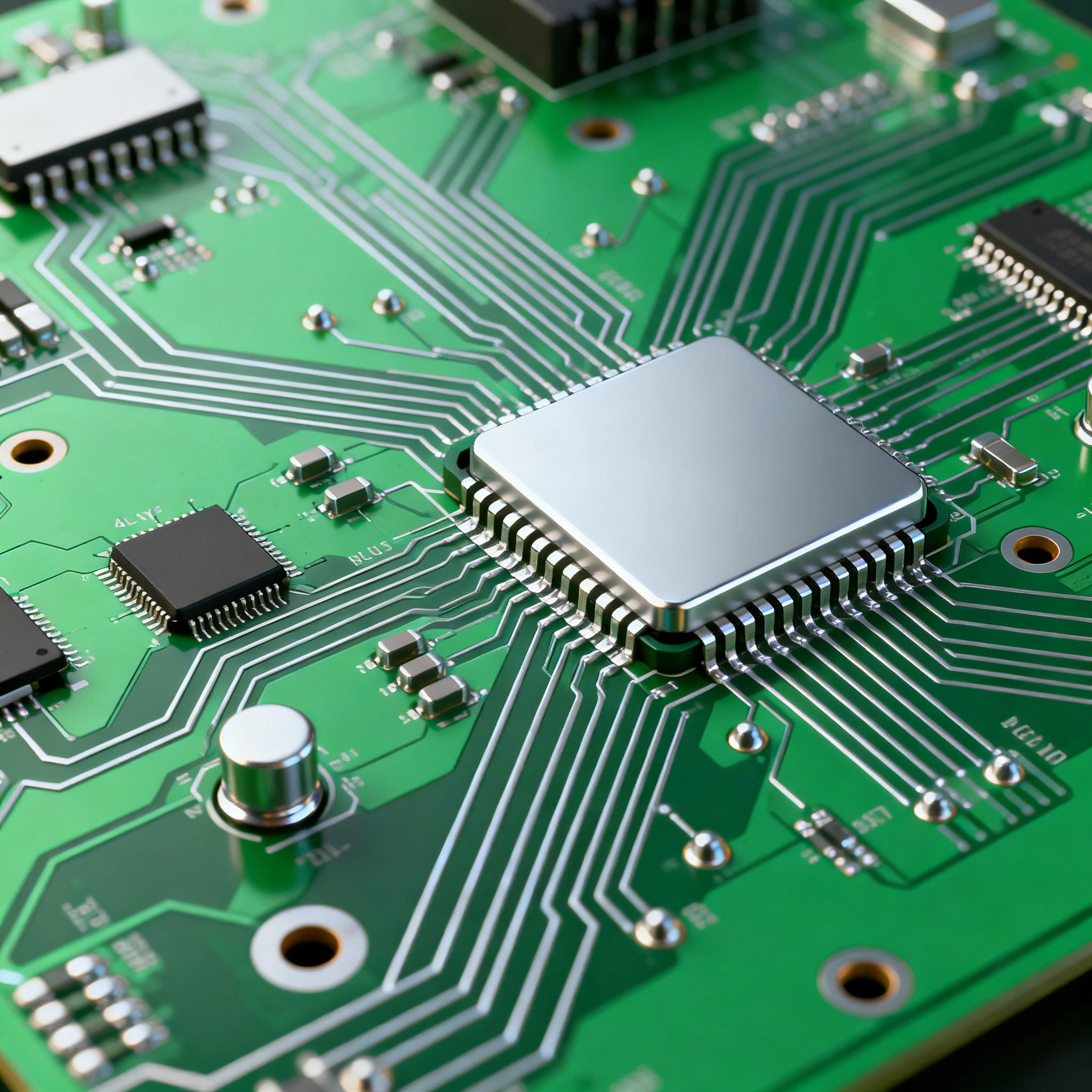
A 4-layer PCB design involves a complex architecture that includes multiple copper planes and insulating layers. The typical structure consists of two outer layers and two inner layers, which can be used for signal routing, power distribution, and ground planes. This architecture offers numerous advantages such as improved signal integrity, reduced electromagnetic interference (EMI), and enhanced thermal management. Understanding the principles of 4-layer PCB design is crucial for achieving optimal performance and reliability in electronic devices.
The core concepts of 4-layer PCB design revolve around efficient layer stack-up, strategic component placement, and meticulous routing. The inner layers are often dedicated to power and ground planes, providing a stable reference for signal layers. This configuration minimizes radiation and crosstalk, ensuring that high-speed signals are transmitted without degradation. Adhering to industry standards such as IPC-A-610 and IPC-2221 ensures that the design meets quality and reliability benchmarks.
In addition to the architectural considerations, selecting the right components is vital. Engineers must carefully evaluate component specifications from datasheets, considering factors such as CPU speed, memory, power requirements, and package type. This ensures compatibility with the design and overall performance goals. The following sections will explore these specifications in detail, providing insights into interpreting and applying them in practical scenarios.
Detailed Specifications
Understanding component specifications is essential for designing effective 4-layer PCBs. These specifications provide crucial information about the performance, compatibility, and limitations of each component. Key parameters include CPU speed, memory capacity, peripheral support, power consumption, and package type. By analyzing these details, engineers can make informed decisions that align with their design objectives and application requirements.
| Specification | Description | Details |
|---|---|---|
| CPU Speed | Maximum operating frequency | 2.5 GHz |
| Memory | RAM capacity | 8 GB DDR4 |
| Peripherals | Supported interfaces | USB 3.0, I2C, SPI |
| Power Supply | Voltage requirements | 3.3V, 5V |
| Package Type | Physical packaging | LQFP-64 |
| Operating Temperature | Temperature range | -40°C to 85°C |
| Storage | Non-volatile memory | 128 GB Flash |
| GPIO | General-purpose I/O pins | 32 pins |
| Clock Speed | Internal clock frequency | 1.2 GHz |
| Power Consumption | Typical current draw | 500 mA |
Key Takeaways from the Specifications
The core specifications outlined above provide a comprehensive view of the component's capabilities and limitations. The CPU speed of 2.5 GHz indicates a high-performance processor suitable for demanding applications, while the 8 GB DDR4 memory ensures efficient multitasking. The variety of supported peripherals, including USB 3.0, I2C, and SPI, allows for versatile connectivity options. Understanding the power supply requirements is crucial for designing a stable power distribution network, while the LQFP-64 package type emphasizes the importance of considering physical dimensions and footprint compatibility in the PCB layout. Engineers must balance these specifications with the intended application, ensuring that the selected components align with the overall design goals.
| Characteristic | Parameter | Value |
|---|---|---|
| Operating Voltage | Vcc | 3.3V |
| Input Current | Icc | 150 mA |
| Output Voltage | Vo | 5V |
| Input Leakage Current | Ileak | 5 µA |
| Output Current | Io | 100 mA |
| Propagation Delay | tPD | 10 ns |
| Rise Time | tr | 5 ns |
| Fall Time | tf | 5 ns |
| ESD Protection | Voltage | 2 kV |
| Power Dissipation | Pd | 1 W |
Practical Implications
The electrical characteristics table provides vital insights into the component's operational parameters. The operating voltage of 3.3V is common in modern electronics, ensuring compatibility with a wide range of devices. The input and output current ratings highlight the component's power handling capabilities, which are crucial for designing robust power distribution networks. Propagation delay and rise/fall times are critical for high-speed applications, as they impact signal integrity and timing. ESD protection of 2 kV ensures resilience against electrostatic discharge, a common issue in electronics. Engineers must consider these characteristics when designing circuits to ensure optimal performance and reliability.
| Application | Configuration | Details |
|---|---|---|
| Consumer Electronics | High performance | Smartphones, tablets |
| Industrial Automation | Robust design | PLC controllers, sensors |
| Automotive | High reliability | ECUs, infotainment systems |
| Medical Devices | Precision | Diagnostic equipment, monitors |
| IoT Devices | Low power | Smart home devices, wearables |
| Telecommunications | High bandwidth | Routers, modems |
Application Guidelines
The application comparison table illustrates the diverse use cases for 4-layer PCB designs. In consumer electronics, high-performance configurations are essential for devices like smartphones and tablets, where processing power and efficiency are paramount. Industrial automation applications demand robust designs capable of withstanding harsh environments, making them ideal for PLC controllers and sensors. Automotive applications prioritize high reliability, crucial for ECUs and infotainment systems. Medical devices require precision and accuracy, while IoT devices benefit from low power configurations to extend battery life. Telecommunications applications demand high bandwidth to support fast data transfer rates. Understanding these application guidelines helps engineers tailor their designs to meet specific industry requirements.
Design Considerations
Designing a 4-layer PCB requires careful consideration of several factors to ensure optimal performance and reliability. One of the most critical aspects is the layer stack-up, which should be strategically configured to minimize crosstalk and EMI. Typically, the inner layers are dedicated to power and ground planes, providing a stable reference for signal layers. This configuration helps reduce radiation and improve signal integrity.
Component placement is another vital consideration. Placing components with high-speed signals close to each other can reduce trace lengths and minimize signal delay. It's also essential to consider thermal management, especially in high-power applications. Utilizing thermal vias and heat sinks can help dissipate heat effectively, preventing overheating and ensuring longevity.
Routing is a crucial aspect of PCB design. Using differential pairs for high-speed signals can improve noise immunity and signal quality. It's essential to follow design rules and guidelines from PCB fabrication resources such as PCBWay and Nova PCBA to ensure manufacturability and compliance with industry standards.
Finally, engineers should conduct thorough design reviews and simulations to identify potential issues early in the design process. This proactive approach can save time and resources by preventing costly redesigns and ensuring a smooth transition from design to manufacturing.
Step-by-Step Implementation
- Define Requirements: Start by defining the design requirements, including performance targets, environmental considerations, and regulatory compliance. This step sets the foundation for the entire design process.
- Select Components: Based on the defined requirements, select suitable components that meet the performance and compatibility criteria. Refer to datasheets and specifications to ensure optimal component selection.
- Design Schematic: Create a detailed schematic diagram that outlines the electrical connections between components. Use schematic capture software to ensure accuracy and consistency.
- Configure Layer Stack-Up: Define the layer stack-up for the PCB, considering power and ground plane placement, signal layers, and thermal management. Refer to IPC standards for guidance.
- Place Components: Strategically place components on the PCB layout, considering factors such as signal integrity, thermal management, and manufacturability. Use design software to optimize placement.
- Route Traces: Route the electrical traces, following best practices for signal integrity and minimizing EMI. Pay attention to trace widths, lengths, and impedance matching for high-speed signals.
- Conduct Design Review: Perform a thorough design review to identify potential issues and ensure compliance with design rules. Use simulation tools to validate signal integrity and thermal performance.
- Generate Manufacturing Files: Once the design is finalized, generate the necessary manufacturing files, including Gerber files, bill of materials (BOM), and assembly drawings. Submit these files to a trusted PCB manufacturer for fabrication and assembly.
Common Issues & Solutions
- Signal Integrity Problems: Signal integrity issues can arise from improper trace routing or impedance mismatches. To resolve this, ensure that traces are properly routed with controlled impedance and minimize stubs and vias.
- Electromagnetic Interference (EMI): EMI can disrupt circuit operation and degrade performance. Use proper grounding techniques, shield sensitive components, and follow best practices for routing high-speed signals.
- Thermal Management Issues: Overheating can lead to component failure and reduced reliability. Implement thermal vias, heat sinks, and proper airflow to dissipate heat effectively.
- Power Distribution Network (PDN) Issues: Inadequate power distribution can result in voltage drops and instability. Use decoupling capacitors and ensure proper power and ground plane design to maintain a stable PDN.
- Manufacturing Defects: Common manufacturing defects include solder bridging and misalignment. Work closely with your PCB manufacturer to ensure adherence to design rules and perform thorough inspections and testing post-assembly.
Applications & Use Cases
4-layer PCBs find applications across various industries due to their versatility and performance advantages. In consumer electronics, they are used in smartphones and tablets to accommodate high-speed processing and compact designs. Industrial automation benefits from their robust construction, making them suitable for PLC controllers and sensors. The automotive industry relies on 4-layer PCBs for critical applications like ECUs and infotainment systems, where reliability is paramount. Medical devices leverage their precision for diagnostic equipment and monitors. IoT devices utilize low power configurations to extend battery life, while telecommunications applications demand high bandwidth capabilities for routers and modems.
Selection & Sourcing Guide
Selecting and sourcing components for 4-layer PCB designs requires careful consideration of performance specifications, compatibility, and availability. Engineers should refer to comprehensive databases such as IC Online to find detailed component information and supplier options. Comparing datasheets and evaluating supplier reliability are crucial steps in ensuring that the selected components meet design requirements and are available for production.
FAQ
- What is the advantage of a 4-layer PCB over a 2-layer PCB? A 4-layer PCB offers improved signal integrity, reduced EMI, and enhanced thermal management compared to a 2-layer PCB, making it suitable for high-performance applications.
- How do I determine the appropriate layer stack-up for my design? Consider the application's signal integrity, power distribution, and thermal management needs to define an optimal layer stack-up. Utilize industry standards and design software for guidance.
- What are the key factors to consider when selecting components? Consider factors such as CPU speed, memory capacity, power requirements, and package type to ensure compatibility with your design and performance goals.
- How can I minimize EMI in my PCB design? Use proper grounding techniques, shield sensitive components, and follow best practices for routing high-speed signals to minimize EMI.
- What role do power and ground planes play in a 4-layer PCB? Power and ground planes provide a stable reference for signal layers, reducing radiation and crosstalk while ensuring reliable power distribution.
- How do I address thermal management issues in my design? Implement thermal vias, heat sinks, and proper airflow to dissip