Mastering Multilayer PCB Stack-Up Design: Key Considerations and Examples
Mastering Multilayer PCB Stack-Up Design: Key Considerations and Examples table { border-collapse: collapse; width: 100%; margin: 20px 0; } table, th, td { border: 1px solid #ccc; padding: 8px; } thea...
Introduction
In the rapidly evolving electronics industry, mastering multilayer PCB stack-up design is crucial for engineers aiming to optimize performance and reliability. As devices become more compact and complex, the demand for efficient multilayer PCBs has surged. These PCBs are essential for high-speed applications, enabling better signal integrity and power distribution. Understanding the nuances of multilayer stack-up design can significantly impact the performance and manufacturability of electronic devices, making it an indispensable skill for modern electronics engineers.
Technical Overview
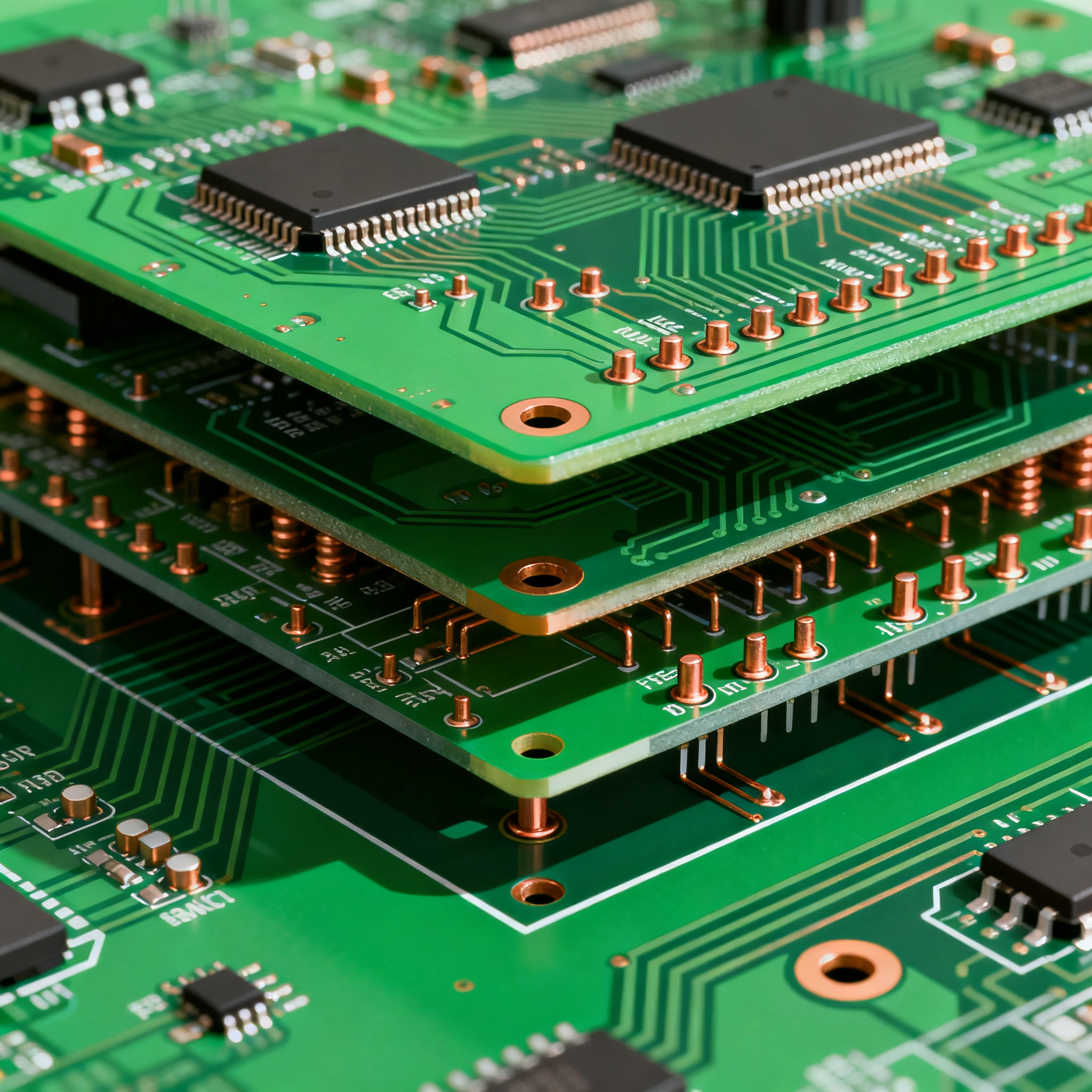
Multilayer PCB stack-up design involves arranging multiple layers of conductive and insulating materials to form a cohesive circuit board. This design is critical in addressing issues like electromagnetic interference (EMI), signal integrity, and thermal management. The core concepts include defining the number of layers, selecting appropriate materials, and determining the optimal layer sequence. Each layer serves a specific function, such as power distribution, ground planes, or signal routing. Proper stack-up design enhances electrical performance, reduces crosstalk, and provides mechanical stability.
The architecture of a multilayer PCB typically consists of alternating layers of conductive copper and insulating dielectric materials. The principles guiding this design include minimizing loop areas, ensuring adequate impedance control, and providing robust grounding. By adhering to these principles, engineers can achieve a balanced design that meets both electrical and mechanical requirements.
Detailed Specifications
When designing multilayer PCBs, certain specifications are paramount. These include layer count, material selection, trace width and spacing, and impedance control. Understanding these parameters and their impact on performance is essential for creating efficient and reliable PCBs. Accurate calculations and adherence to industry standards, such as IPC-A-610 and IPC-2221, ensure that designs meet quality and performance criteria.
| Parameter | Value | Formula/Calculation |
|---|---|---|
| Layer Count | 4 | N/A |
| Trace Width | 0.2 mm | Based on current capacity |
| Impedance | 50 Ohms | Z = 87 / sqrt(εr) * ln(5.98h/(0.8W + T)) |
| Dielectric Constant (εr) | 4.2 | N/A |
| Layer Thickness | 1.6 mm | Total stack-up thickness |
| Signal Layer | 2 | N/A |
| Ground Layer | 1 | N/A |
| Power Layer | 1 | N/A |
| Clearance | 0.15 mm | IPC-2221 standard |
| Copper Weight | 1 oz | N/A |
Key Takeaways from the Specifications
The detailed specifications table provides a snapshot of critical design parameters for a multilayer PCB. The layer count, trace width, and impedance are vital for determining the board's electrical performance. For instance, maintaining a 50 Ohm impedance is crucial for high-speed signal integrity. The dielectric constant and layer thickness influence the board's mechanical and thermal properties. Adhering to IPC standards ensures reliability and manufacturability. Understanding these specifications helps in optimizing design for both performance and cost.
| Performance Metric | Value | Remarks |
|---|---|---|
| Gain | 10 dB | Amplification factor |
| Bandwidth | 2 GHz | Frequency range |
| Noise Figure | 3 dB | Signal-to-noise ratio |
| Power Consumption | 5 W | Total power use |
| Signal Integrity | High | Minimal crosstalk |
| Thermal Resistance | 20 °C/W | Heat dissipation |
| EMI | Low | Electromagnetic interference |
| Reliability | High | Long-term performance |
| Latency | 1 ns | Signal delay |
Practical Implications
The performance analysis table highlights crucial metrics that define the operational efficiency of a multilayer PCB. Gain and bandwidth are key indicators of the board's capability to handle high-speed signals. A low noise figure and minimal EMI contribute to superior signal integrity, while power consumption and thermal resistance are critical for energy efficiency and heat management. These metrics guide engineers in refining designs to meet specific application requirements, ensuring both performance and reliability.
| Configuration | Pros | Cons |
|---|---|---|
| 4-Layer | Cost-effective, simple design | Limited routing |
| 6-Layer | Improved signal integrity | Higher cost |
| 8-Layer | Excellent EMI control | Complex manufacturing |
| 10-Layer | High density, advanced designs | Expensive |
| FR-4 Material | Widely available, affordable | Limited high-frequency performance |
| Rogers Material | Superior high-frequency performance | Costly |
| Thin Core | Compact design | More susceptible to warping |
| Thick Core | Stable, robust | Increased weight |
Application Guidelines
When selecting a multilayer PCB configuration, understanding the trade-offs is crucial. A 4-layer stack-up may be cost-effective but limits routing options, whereas an 8-layer design offers excellent EMI control at a higher cost. Material choice, such as FR-4 versus Rogers, impacts performance and budget. Core thickness affects the board's mechanical stability and size. These considerations help in tailoring the PCB design to specific application needs, balancing performance, cost, and manufacturability.
Design Considerations
Designing a multilayer PCB requires careful consideration of various factors to achieve optimal performance. Key considerations include:
- Layer Count and Arrangement: Determine the number of layers based on the complexity of the circuit. More layers allow for better separation of power and signal paths, reducing interference.
- Material Selection: Choose materials that provide the necessary electrical and thermal properties. FR-4 is common for general applications, while Rogers materials are preferred for high-frequency designs.
- Trace Width and Spacing: Ensure proper trace dimensions to handle the required current and prevent signal loss. Adhere to IPC standards for reliability.
- Impedance Control: Design traces with controlled impedance to maintain signal integrity, especially in high-speed applications.
- Thermal Management: Incorporate thermal vias and heat sinks to dissipate heat efficiently, preventing component damage.
- Mechanical Stability: Consider core thickness and material properties to ensure the board can withstand mechanical stress during assembly and operation.
By addressing these considerations, engineers can design multilayer PCBs that meet both performance and reliability standards, tailored to specific application requirements.
Step-by-Step Implementation
Implementing a multilayer PCB design involves several critical steps:
- Define Requirements: Begin by outlining the functional and performance requirements of the PCB, including signal types, power levels, and environmental conditions.
- Select Materials: Choose appropriate materials for the dielectric and conductive layers based on the application's electrical, thermal, and mechanical needs.
- Design Stack-Up: Plan the layer arrangement, assigning specific functions to each layer (e.g., power, ground, signal) to optimize performance.
- Perform Calculations: Calculate trace widths, spacing, and impedance using industry-standard formulas to ensure compliance with design specifications.
- Layout Design: Use PCB design software to create the layout, incorporating components, traces, and vias based on the stack-up plan.
- Simulate Performance: Conduct simulations to assess signal integrity, thermal performance, and EMI, making adjustments as needed.
- Prototype and Test: Manufacture a prototype PCB and perform thorough testing to validate the design against requirements.
- Finalize Design: Make any necessary revisions based on testing results, then finalize the design for production, ensuring all documentation is complete.
Following these steps ensures a systematic approach to multilayer PCB design, leading to a robust and reliable end product.
Common Issues & Solutions
Designing multilayer PCBs can present several common challenges. Here are some issues and their solutions:
- Signal Integrity Issues: Poor signal integrity can result from inadequate impedance control. Solution: Use controlled impedance traces and maintain consistent trace width and spacing.
- Thermal Management Problems: Excessive heat can damage components. Solution: Incorporate thermal vias and heat sinks, and use materials with good thermal conductivity.
- EMI Concerns: Electromagnetic interference can degrade performance. Solution: Implement proper grounding techniques and use shielded traces.
- Mechanical Stability Issues: Warping and bending can occur. Solution: Opt for thicker cores and materials with high mechanical strength.
- Manufacturing Defects: Misalignment and layer delamination can occur during production. Solution: Work with reputable manufacturers and adhere to IPC standards for quality control.
Addressing these issues early in the design process helps prevent costly revisions and ensures a successful PCB implementation.
Applications & Use Cases
Multilayer PCBs are widely used in various applications due to their ability to handle complex circuits and high-speed signals. Common use cases include:
- Consumer Electronics: Smartphones, tablets, and laptops utilize multilayer PCBs for compact and efficient designs.
- Telecommunications: Networking equipment and communication devices rely on multilayer PCBs for high-speed data transmission.
- Automotive Electronics: Advanced driver-assistance systems (ADAS) and infotainment systems require robust multilayer PCBs for reliability and performance.
- Medical Devices: Diagnostic and monitoring equipment use multilayer PCBs for precise and reliable operation.
- Aerospace and Defense: Complex avionics and defense systems benefit from the performance and reliability of multilayer PCBs.
These applications highlight the versatility and importance of multilayer PCB designs across various industries.
Selection & Sourcing Guide
Selecting and sourcing the right components and materials for multilayer PCBs is critical for achieving desired performance. Engineers should consider:
- Specification Compliance: Ensure components meet the required electrical, thermal, and mechanical specifications.
- Supplier Reliability: Choose suppliers with a proven track record for quality and timely delivery.
- Cost-Effectiveness: Balance performance requirements with budget constraints, opting for cost-effective solutions without compromising quality.
For sourcing components, visit IC Online for a wide range of electronic components and materials.
FAQ
- What is the primary advantage of multilayer PCBs? Multilayer PCBs offer enhanced signal integrity, reduced EMI, and greater routing capabilities, making them ideal for complex and high-speed applications.
- How do I determine the number of layers needed for my PCB? The layer count depends on the circuit's complexity, signal integrity requirements, and space constraints. More layers provide better separation and routing options.
- What materials are commonly used in multilayer PCBs? FR-4 is a standard material for general applications, while Rogers materials are used for high-frequency designs due to their superior electrical properties.
- How can I ensure good thermal management in my PCB design? Use thermal vias, heat sinks, and materials with high thermal conductivity to efficiently dissipate heat and prevent component damage.
- What role does impedance control play in PCB design? Impedance control is crucial for maintaining signal integrity, especially in high-speed applications, by minimizing reflections and signal loss.
- How can I minimize EMI in my multilayer PCB? Implement proper grounding techniques, use shielded traces, and design the stack-up to minimize loop areas and crosstalk.
- Why is mechanical stability important in PCB design? Mechanical stability ensures the PCB can withstand stress during assembly and operation, preventing warping and damage.
- What are some common manufacturing issues with multilayer PCBs? Common issues include misalignment, layer delamination, and defects due to poor quality control. Work with reputable manufacturers to mitigate these risks.
- How do I choose the right PCB manufacturer? Consider factors such as manufacturing capabilities, quality standards adherence, turnaround time, and cost when selecting a manufacturer.
- Can multilayer PCBs be used in harsh environments? Yes, with proper material selection and design considerations, multilayer PCBs can be made to withstand harsh environmental conditions.
Conclusion
Mastering multilayer PCB stack-up design is essential for engineers looking to optimize the performance and reliability of electronic devices. By understanding the key design parameters, performance metrics, and trade-offs, engineers can create efficient and robust PCB designs tailored to specific applications. Adhering to industry standards and leveraging advanced materials and techniques further enhances the design process, ensuring success in the ever-evolving electronics landscape.