Mastering Multilayer PCB Stack-Up Design: A Cost-Effective Guide for Optimal Performance
Mastering Multilayer PCB Stack-Up Design Introduction In the ever-evolving world of electronics, mastering multilayer PCB stack-up design is crucial for engineers looking to optimize performance while...
Introduction
In the ever-evolving world of electronics, mastering multilayer PCB stack-up design is crucial for engineers looking to optimize performance while maintaining cost-effectiveness. As electronic devices become more complex, the demand for efficient and reliable PCB designs has never been higher. Understanding the intricacies of multilayer PCB stack-ups not only enhances signal integrity and thermal management but also plays a significant role in reducing electromagnetic interference (EMI). This guide delves into the key aspects of multilayer PCB stack-up design, providing engineers with the knowledge needed to make informed design choices that meet industry standards and application requirements.
Technical Overview
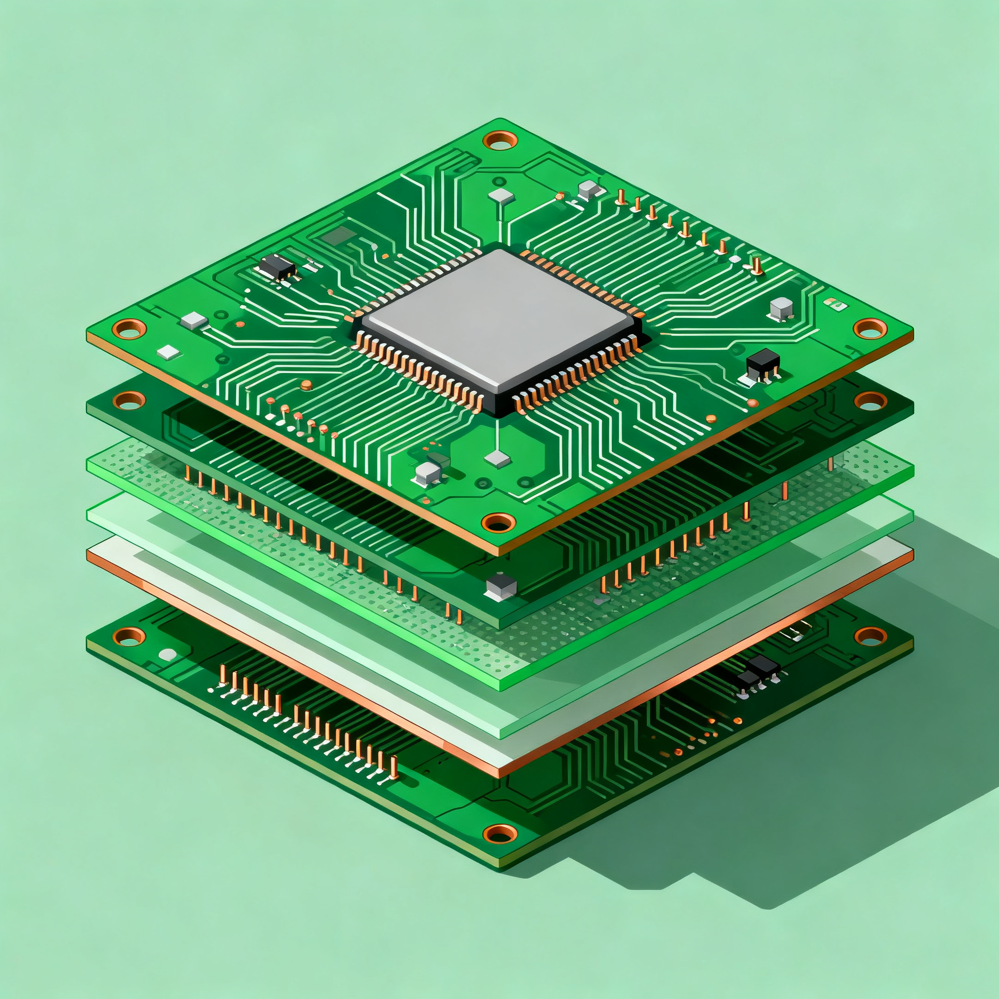
Multilayer PCB stack-up design involves the strategic arrangement of conductive and insulating layers within a printed circuit board. This architecture is fundamental in supporting the electrical and mechanical functions of modern electronic devices. The primary goal is to enhance electrical performance while minimizing the board's size and weight. Key concepts include:
- Signal Integrity: Ensuring that signals are transmitted with minimal distortion or loss.
- Power Distribution: Efficiently managing power delivery across the board to prevent voltage drops and power losses.
- Thermal Management: Implementing strategies to dissipate heat effectively and maintain optimal operating temperatures.
- Electromagnetic Compatibility (EMC): Designing to reduce EMI and ensure compliance with regulatory standards.
Proper stack-up design also involves considerations for manufacturing processes, such as layer alignment and via design, which are critical for maintaining the board's structural integrity and functionality.
Detailed Specifications
Understanding key specifications is vital in multilayer PCB stack-up design. These specifications provide insights into the board's capabilities and limitations, guiding engineers in making informed decisions. Important specifications include layer count, material type, dielectric thickness, and copper weight. These parameters influence the board's electrical performance, thermal management, and mechanical robustness.
| Parameter | Description | Typical Values |
|---|---|---|
| Layer Count | Number of conductive layers | 4 to 16 layers |
| Material Type | Base material used for the PCB | FR-4, Rogers 4350 |
| Dielectric Thickness | Thickness of insulating layers | 0.1mm to 0.5mm |
| Copper Weight | Thickness of copper layers | 0.5 oz to 2 oz |
| Impedance Control | Specified characteristic impedance | 50 Ohms ± 10% |
| Thermal Conductivity | Ability to conduct heat | 0.8 W/mK to 1.5 W/mK |
| Operating Temperature | Temperature range for operation | -40°C to 125°C |
| Via Types | Types of vias used | Through-hole, Blind, Buried |
| Solder Mask Type | Type of protective layer | Green, Black, Blue |
| Surface Finish | Coating applied to copper pads | HASL, ENIG, OSP |
| Board Thickness | Total thickness of the PCB | 0.6mm to 3.2mm |
| Signal Layer Count | Number of layers dedicated to signals | 2 to 10 layers |
Key Takeaways from the Specifications
The data in Table 1 highlights the critical parameters that define a multilayer PCB's capabilities. For instance, the layer count directly impacts the board's complexity and potential routing capacity. Material type influences both electrical performance and thermal management. Dielectric thickness and copper weight are crucial for impedance control and thermal conductivity, respectively. Understanding these specifications allows engineers to tailor their designs to meet specific application needs, ensuring optimal performance and reliability.
| Metric | Description | Typical Values |
|---|---|---|
| Signal Loss | Attenuation of signal strength | 0.1 dB/in to 0.5 dB/in |
| Dielectric Constant | Relative permittivity of the material | 3.5 to 4.2 |
| Thermal Resistance | Resistance to heat flow | 0.5°C/W to 1.2°C/W |
| Crosstalk | Unwanted coupling of signals | < 5% |
| Insertion Loss | Loss of signal power | 0.2 dB/in to 0.8 dB/in |
| Return Loss | Reflection of signal power | 10 dB to 20 dB |
| Frequency Range | Operational frequency range | DC to 10 GHz |
| Current Carrying Capacity | Maximum current per trace | 1A to 3A |
| Thermal Expansion | Material expansion due to heat | 14 ppm/°C to 18 ppm/°C |
| Flexural Strength | Resistance to bending | 100 MPa to 150 MPa |
Practical Implications
The performance metrics in Table 2 provide insight into the electrical and thermal characteristics of multilayer PCBs. Signal loss and insertion loss are critical for high-frequency applications, affecting the board's ability to maintain signal integrity. Thermal resistance and thermal expansion are key for thermal management, ensuring the PCB can operate safely under varying temperature conditions. Engineers must consider these metrics during design to optimize performance and prevent issues such as crosstalk or signal degradation.
| Use Case | Configuration | Benefits |
|---|---|---|
| High-Speed Digital | 8-layer, FR-4, Controlled Impedance | Reduced signal loss, improved EMI |
| RF and Microwave | 10-layer, Rogers 4350, Low DK | Low insertion loss, high frequency stability |
| Automotive | 6-layer, High Tg FR-4, Thick Copper | Enhanced thermal management, robustness |
| Consumer Electronics | 4-layer, Standard FR-4, Solder Mask | Cost-effective, reliable performance |
| Industrial Control | 12-layer, Mixed Dielectrics, Blind Vias | Complex routing, high reliability |
| Telecommunications | 16-layer, Hybrid Materials, High-Speed | High data rates, superior signal integrity |
| Medical Devices | 8-layer, Biocompatible, ENIG Finish | Safe for medical use, corrosion resistance |
| Aerospace | 14-layer, Polyimide, Lightweight | High temperature tolerance, weight savings |
Application Guidelines
The application matrix in Table 3 illustrates the diverse use cases and configurations for multilayer PCBs. Each application, from high-speed digital to aerospace, has specific requirements that influence the choice of materials, layer count, and design features. Understanding these configurations helps engineers select the appropriate stack-up to meet performance goals and regulatory standards, ensuring the final product is both efficient and compliant.
Design Considerations
Designing a multilayer PCB stack-up involves several critical considerations to ensure optimal performance and manufacturability. Key factors include:
- Layer Arrangement: Strategic placement of power, ground, and signal layers to minimize EMI and enhance signal integrity.
- Impedance Control: Precise calculation and implementation of trace widths and spacing to maintain the desired impedance across high-speed signals.
- Thermal Management: Integration of thermal vias and heat sinks to dissipate heat effectively, preventing overheating and ensuring reliability.
- Material Selection: Choosing materials with appropriate dielectric constants and thermal properties to meet application-specific requirements.
- Via Design: Utilizing through-hole, blind, and buried vias to optimize signal routing and maintain mechanical strength.
- Manufacturing Constraints: Ensuring the design is compatible with manufacturing capabilities and follows industry standards such as IPC-2221.
- Cost Considerations: Balancing performance requirements with budget constraints to achieve a cost-effective design.
By carefully considering these factors, engineers can create PCB designs that meet performance goals while remaining within budget and manufacturing constraints.
Step-by-Step Implementation
- Define Requirements: Start by defining the electrical, thermal, and mechanical requirements of the PCB based on the application.
- Select Materials: Choose materials with suitable dielectric constants, thermal properties, and mechanical strength.
- Determine Layer Count: Decide on the number of layers needed to accommodate all signals, power, and ground planes.
- Design Stack-Up: Arrange layers strategically to optimize signal integrity, power distribution, and thermal management.
- Calculate Impedance: Use software tools to calculate trace widths and spacing for controlled impedance.
- Implement Thermal Management: Design thermal vias, heat sinks, and other features to manage heat dissipation.
- Review for Manufacturability: Ensure the design meets manufacturing constraints and follows IPC standards.
- Prototype and Test: Create a prototype to test the design's performance and make necessary adjustments.
Following these steps ensures a systematic approach to multilayer PCB design, leading to a reliable and efficient final product.
Common Issues & Solutions
Designing multilayer PCBs can present several challenges. Here are some common issues and their solutions:
- Signal Integrity Issues: Use controlled impedance and proper layer arrangement to minimize signal loss and crosstalk.
- Thermal Management Problems: Implement thermal vias and heat sinks to enhance heat dissipation and prevent overheating.
- EMI Concerns: Design with adequate ground planes and shielding to reduce electromagnetic interference.
- Manufacturing Defects: Ensure design complies with IPC standards and is compatible with manufacturing capabilities.
- Cost Overruns: Balance performance needs with budget constraints by selecting cost-effective materials and design features.
- Complex Routing: Utilize advanced CAD tools and via types to manage complex signal routing effectively.
By addressing these issues proactively, engineers can enhance the reliability and performance of their PCB designs.
Applications & Use Cases
Multilayer PCBs are used in a wide range of applications, each with specific requirements. In the automotive industry, for example, PCBs must withstand harsh environments and provide reliable performance. In telecommunications, high-speed data transmission and signal integrity are critical. Medical devices demand biocompatible materials and precise impedance control. By understanding the unique needs of each application, engineers can tailor their designs to meet specific performance and compliance standards.
Selection & Sourcing Guide
When selecting and sourcing components for multilayer PCBs, engineers should consider factors such as material properties, supplier reliability, and cost. Utilizing resources like IC Online can help identify suitable components and suppliers that meet project requirements and budget constraints.
FAQ
- What is a multilayer PCB? A multilayer PCB is a circuit board with more than two layers of conductive material, allowing for complex circuit designs and improved performance.
- Why is impedance control important? Impedance control ensures consistent signal transmission and prevents reflections and signal loss, especially in high-speed applications.
- How can I improve thermal management? Use thermal vias, heat sinks, and select materials with high thermal conductivity to enhance heat dissipation.
- What materials are commonly used in multilayer PCBs? Common materials include FR-4, Rogers 4350, and polyimide, each offering different electrical and thermal properties.
- What are blind and buried vias? Blind vias connect outer layers to inner layers, while buried vias connect only inner layers, optimizing routing and saving space.
- How do I ensure manufacturability? Follow IPC standards and communicate with manufacturers to ensure the design is compatible with their capabilities.
- What is the role of solder mask? Solder mask protects the PCB from oxidation, prevents solder bridges, and enhances the board's appearance.
- How do I select the right surface finish? Choose based on factors like cost, reliability, and application needs, with options including HASL, ENIG, and OSP.
- What is the impact of layer count on cost? Higher layer counts increase complexity and cost, but they may be necessary for advanced designs requiring more routing capacity.
- How can I reduce EMI? Use ground planes, proper layer stacking, and shielding techniques to minimize electromagnetic interference.
Conclusion
Mastering multilayer PCB stack-up design is essential for engineers seeking to optimize performance and cost-effectiveness. By understanding key specifications, performance metrics, and application guidelines, engineers can create reliable and efficient PCB designs. With careful consideration of design, implementation, and common issues, the path to successful multilayer PCB design becomes clearer. As technology continues to advance, staying informed and adaptable is crucial for achieving success in the dynamic field of electronics engineering.