Mastering Impedance Control in 4-Layer PCBs: Essential Techniques for High-Frequency Applications
Mastering Impedance Control in 4-Layer PCBs Introduction In the rapidly evolving world of electronics, high-frequency applications demand precise control over various parameters to ensure optimal perf...
Introduction
In the rapidly evolving world of electronics, high-frequency applications demand precise control over various parameters to ensure optimal performance. One of the critical factors in PCB design for such applications is impedance control, especially in 4-layer PCBs. Impedance control is essential for maintaining signal integrity, minimizing reflections, and ensuring that the circuit performs as intended. With the increasing demand for faster data rates and more compact designs, mastering impedance control has become more crucial than ever.
Technical Overview
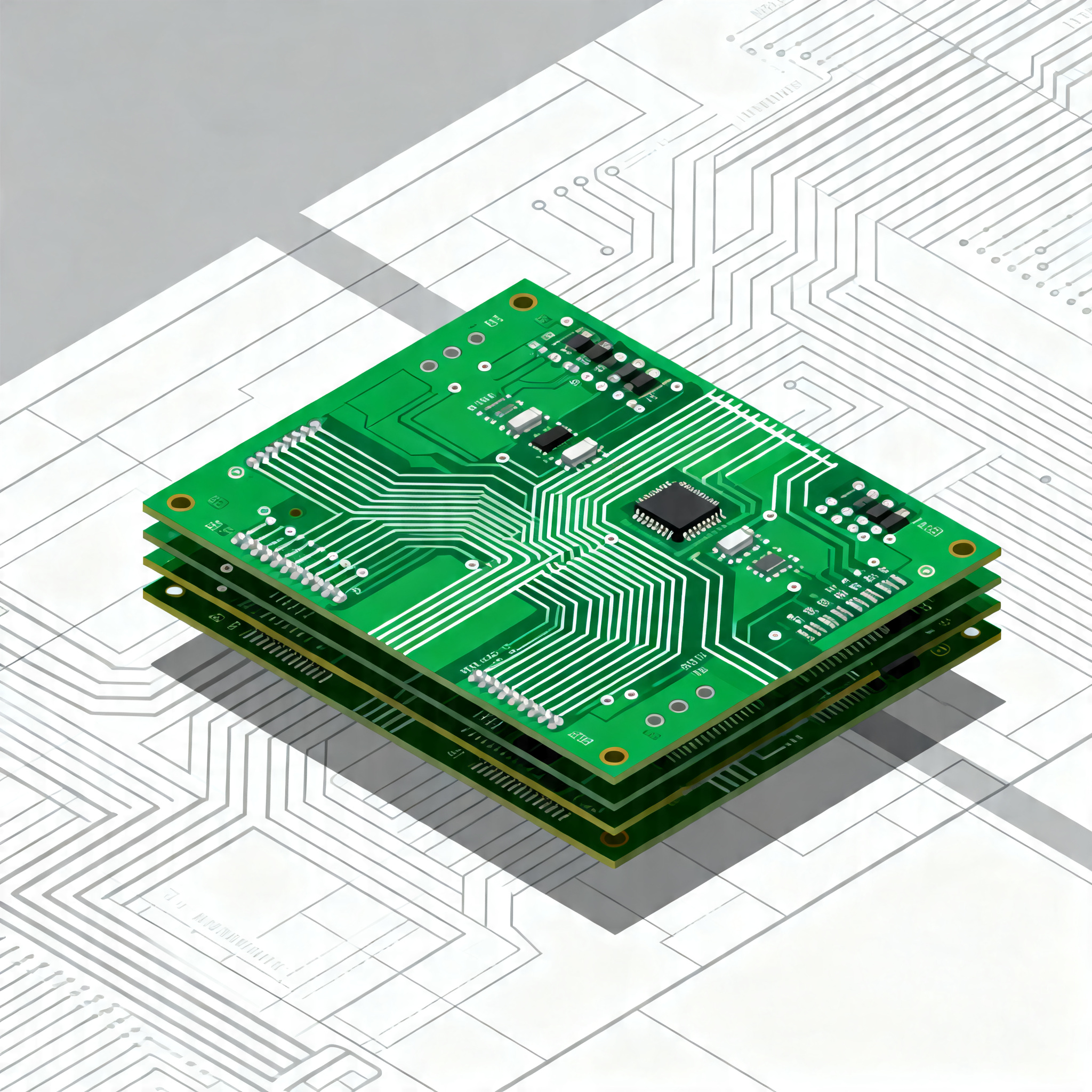
Impedance control in PCBs involves designing the traces and their surrounding environment to have a specific characteristic impedance. This is particularly important in high-frequency applications where signals are transmitted over PCB traces. The architecture of a 4-layer PCB typically includes two inner layers for power and ground planes, which help reduce electromagnetic interference and improve signal integrity. The outer layers are used for routing signals and are designed with controlled impedance to match the impedance of the connected components and transmission lines. Key principles include understanding dielectric materials, trace geometry, and the impact of vias and connectors on impedance.
Detailed Specifications
When selecting components for high-frequency applications, understanding the specifications is crucial. These specifications include CPU speed, memory, power requirements, and package type. Each of these factors can significantly impact the performance and reliability of your design. Below is a detailed table of core specifications for an IC chip commonly used in 4-layer PCB designs.
| Specification | Details | Importance |
|---|---|---|
| CPU Speed | 2.5 GHz | High-speed data processing |
| Memory | 8 GB DDR4 | Fast access for complex tasks |
| Peripherals | USB 3.0, HDMI, PCIe | Versatile connectivity |
| Power Supply | 3.3V, 5V | Standard power levels |
| Package Type | BGA | Compact form factor |
| Operating Temperature | -40°C to 85°C | Wide operational range |
| Storage Temperature | -55°C to 125°C | Safe storage conditions |
| Dimensions | 15mm x 15mm | Space-saving design |
| Weight | 10 grams | Lightweight |
| MTBF | 1,000,000 hours | High reliability |
Key Takeaways from the Specifications
The core specifications table provides insights into the capabilities and limitations of the IC chip. The CPU speed and memory are critical for high-frequency applications, ensuring that data can be processed quickly and efficiently. The power supply requirements highlight the importance of matching the power levels to those available in your PCB design. Additionally, the package type and dimensions are crucial for fitting the component into compact designs. Understanding these specifications helps in selecting the right components that meet the performance and reliability criteria for your application.
Electrical Characteristics
Electrical characteristics define how a component behaves under various electrical conditions. These include voltage levels, current consumption, and timing specifications. These parameters are crucial for ensuring compatibility with other components and maintaining the overall performance of the system. Below is a table detailing the electrical characteristics of the IC chip.
| Characteristic | Value | Significance |
|---|---|---|
| Operating Voltage | 1.8V to 3.3V | Compatibility with power sources |
| Current Consumption | 500 mA | Power efficiency |
| Input Logic Level | 0.8V (Low), 2.0V (High) | Signal integrity |
| Output Logic Level | 0.4V (Low), 2.4V (High) | Signal clarity |
| Propagation Delay | 5 ns | Fast response time |
| Rise/Fall Time | 2 ns | Signal transition speed |
| Input Impedance | 50 Ohms | Matching with transmission lines |
| Output Impedance | 25 Ohms | Drive capability |
| Temperature Coefficient | ±100 ppm/°C | Stability over temperature |
| ESD Protection | 2 kV | Robustness against surges |
Practical Implications
The electrical characteristics table highlights the importance of voltage and current specifications in ensuring compatibility and efficiency in your design. The operating voltage range allows for flexibility in power supply selection, while the current consumption provides insights into the power efficiency of the component. The input and output logic levels are crucial for maintaining signal integrity across the system. Additionally, the propagation delay and rise/fall time are significant for applications requiring fast signal processing. These characteristics must be carefully considered to optimize the performance and reliability of high-frequency applications.
Application Comparison
Different use cases and configurations require specific considerations in terms of impedance control and component selection. The table below compares various applications and their unique requirements.
| Application | Configuration | Requirements |
|---|---|---|
| Wireless Communication | 4-layer PCB | High signal integrity |
| High-Speed Computing | 6-layer PCB | Low power consumption |
| IoT Devices | 2-layer PCB | Compact design |
| Automotive Electronics | 8-layer PCB | High reliability |
| Consumer Electronics | 4-layer PCB | Cost efficiency |
| Aerospace Systems | 10-layer PCB | Extreme temperature tolerance |
| Medical Devices | 6-layer PCB | Precision and accuracy |
| Industrial Automation | 8-layer PCB | Durability |
Application Guidelines
The application comparison table provides a clear overview of how different configurations and requirements influence the design and component selection process. For example, wireless communication applications demand high signal integrity, which is achieved through precise impedance control in 4-layer PCBs. In contrast, high-speed computing applications prioritize low power consumption, often requiring more complex layer configurations. Understanding these unique requirements helps in selecting the appropriate PCB design and components to meet the specific needs of each application, ensuring optimal performance and reliability.
Design Considerations
Designing a 4-layer PCB with controlled impedance requires careful planning and execution. Critical design considerations include selecting the right dielectric materials, optimizing trace geometry, and minimizing the impact of vias and connectors on impedance. The dielectric material determines the propagation speed of signals and affects the characteristic impedance. Trace geometry, including width, spacing, and thickness, must be precisely calculated to achieve the desired impedance. Vias and connectors can introduce impedance discontinuities, so their impact must be minimized through careful placement and design. Additionally, maintaining a consistent reference plane and using proper grounding techniques are essential for reducing electromagnetic interference and ensuring signal integrity. By adhering to these design considerations, engineers can effectively manage impedance and optimize the performance of high-frequency applications.
Step-by-Step Implementation
Implementing impedance control in a 4-layer PCB involves several detailed steps. First, define the design requirements, including the desired impedance and signal integrity specifications. Next, select suitable dielectric materials and calculate the trace geometry to achieve the target impedance. Use simulation tools to model the PCB layout and verify the impedance control. During the layout phase, ensure that traces are routed with consistent widths and spacing, and avoid sharp bends that can cause impedance discontinuities. Place vias and connectors strategically to minimize their impact on impedance. Once the design is finalized, conduct thorough testing and validation to ensure that the PCB meets the performance criteria. If necessary, make adjustments to the design based on test results. Finally, document the design and manufacturing process to ensure reproducibility and quality control. By following these steps, engineers can successfully implement impedance control in 4-layer PCBs for high-frequency applications.
Common Issues & Solutions
Impedance control in 4-layer PCBs can present several challenges. One common issue is impedance mismatch, which can cause signal reflections and degrade performance. This can be addressed by accurately calculating and matching the impedance of traces and components. Another issue is electromagnetic interference, which can be minimized by maintaining a consistent reference plane and using proper grounding techniques. Vias and connectors can introduce impedance discontinuities, so their placement and design must be carefully managed. Signal integrity issues can also arise from improper trace routing, which can be resolved by maintaining consistent trace geometry and avoiding sharp bends. Additionally, thermal management is crucial in high-frequency applications, and can be addressed by using appropriate materials and design techniques. By understanding and addressing these common issues, engineers can ensure the successful implementation of impedance control in their PCB designs.
Applications & Use Cases
Impedance control in 4-layer PCBs is critical for a wide range of high-frequency applications. In wireless communication, precise impedance control ensures high signal integrity and reliable data transmission. In high-speed computing, low power consumption and efficient signal processing are achieved through careful impedance management. IoT devices benefit from compact designs and cost efficiency, while automotive electronics require high reliability and durability. Aerospace systems demand extreme temperature tolerance, and medical devices require precision and accuracy. By understanding the specific requirements of each application, engineers can design and implement PCB solutions that meet the unique needs of these diverse use cases.
Selection & Sourcing Guide
Selecting the right components for impedance-controlled 4-layer PCBs involves considering specifications such as CPU speed, memory, power requirements, and package type. It's essential to source components from reliable suppliers to ensure quality and compatibility. For more information on component selection and sourcing, visit IC Online. This platform provides a comprehensive database of electronic components, datasheets, and sourcing options to help engineers make informed decisions and streamline the design process.
FAQ
Q1: What is impedance control in PCBs?
A1: Impedance control is the practice of designing PCB traces and their environment to have a specific characteristic impedance, crucial for high-frequency signal integrity.
Q2: Why is impedance control important in 4-layer PCBs?
A2: It ensures consistent signal integrity, minimizes reflections, and enhances performance in high-frequency applications.
Q3: How do dielectric materials affect impedance control?
A3: Dielectric materials influence the propagation speed of signals and the characteristic impedance of traces.
Q4: What role do vias play in impedance control?
A4: Vias can introduce impedance discontinuities, so their impact must be minimized through careful design and placement.
Q5: How can I ensure signal integrity in high-frequency applications?
A5: Maintain consistent trace geometry, use proper grounding techniques, and minimize electromagnetic interference.
Q6: What are the common challenges in impedance control?
A6: Impedance mismatch, electromagnetic interference, and signal integrity issues are common challenges that can be addressed through careful design.
Q7: How do I select components for impedance-controlled PCBs?
A7: Consider specifications such as CPU speed, memory, power requirements, and package type to ensure compatibility and performance.
Q8: Where can I find reliable component sourcing options?
A8: Visit IC Online for a comprehensive database of electronic components and sourcing options.
Conclusion
Mastering impedance control in 4-layer PCBs is essential for achieving optimal performance in high-frequency applications. By understanding the core specifications, electrical characteristics, and application requirements, engineers can design and implement effective PCB solutions. Addressing common challenges and leveraging reliable component sourcing options ensures that designs meet the unique needs of diverse applications, from wireless communication to medical devices. With careful planning and execution, impedance control can be successfully integrated into PCB designs to enhance signal integrity and reliability.