Mastering Impedance Control for 4-Layer PCBs: Essential Techniques for Optimal Performance
Mastering Impedance Control for 4-Layer PCBs: Essential Techniques for Optimal Performance body { font-family: Arial, sans-serif; line-height: 1.6; margin: 0; padding: 20px; } h2 { color: #333; } tabl...
Introduction
In the world of electronics, printed circuit boards (PCBs) are the backbone of any electronic device. With the ever-increasing demand for faster and more efficient devices, mastering impedance control in multi-layer PCBs, especially 4-layer ones, has become crucial. Impedance control is vital for maintaining signal integrity, reducing electromagnetic interference (EMI), and ensuring optimal performance. This article delves into the essential techniques and considerations for achieving effective impedance control in 4-layer PCBs, focusing on component specifications, application circuits, and design guidelines.
Technical Overview
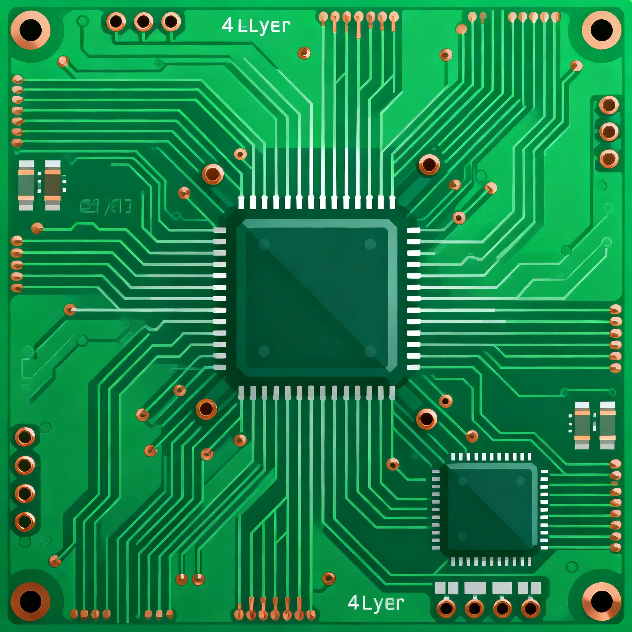
Impedance control is a critical aspect of PCB design that ensures signals are transmitted without degradation across the board. It involves managing the characteristic impedance of traces, which is determined by the trace width, height above the ground plane, and the dielectric material's properties. For 4-layer PCBs, the architecture typically includes a signal layer, ground plane, power plane, and another signal layer. This configuration allows for enhanced signal integrity and power distribution. Understanding the principles of controlled impedance, such as characteristic impedance, differential impedance, and the role of dielectric materials, is essential for designing effective 4-layer PCBs.
Detailed Specifications
When designing a 4-layer PCB with controlled impedance, several key specifications must be considered. These include trace width and spacing, dielectric constant, and board thickness. These parameters are crucial as they directly affect the impedance values and, consequently, the performance of the PCB. Proper documentation and adherence to standards like IPC-2221 are essential for ensuring that these specifications are met.
| Parameter | Specification | Importance |
|---|---|---|
| Trace Width | 5-10 mils | Determines impedance |
| Dielectric Constant | 4.2-4.7 | Affects signal speed |
| Board Thickness | 1.6 mm | Structural stability |
| Layer Stackup | Signal-Ground-Power-Signal | Signal integrity |
| Copper Thickness | 1 oz | Conductivity |
| Impedance Tolerance | ±10% | Consistency |
| Via Diameter | 0.2 mm | Connection reliability |
| Surface Finish | ENIG | Corrosion resistance |
| Minimum Solder Mask Clearance | 0.1 mm | Avoid short circuits |
| Maximum Operating Temperature | 105°C | Thermal stability |
Key Takeaways from the Specifications
The specifications outlined in the table provide a foundation for ensuring that 4-layer PCBs meet the necessary performance standards. Trace width and dielectric constant are pivotal in determining the board's impedance, impacting signal integrity. The layer stackup configuration, such as Signal-Ground-Power-Signal, is essential for maintaining signal integrity and minimizing EMI. Copper thickness and surface finish like ENIG ensure the board's durability and longevity. Understanding these specifications allows designers to make informed decisions that enhance PCB performance and reliability.
| Metric | Value | Significance |
|---|---|---|
| Characteristic Impedance | 50 Ω | Signal integrity |
| Insertion Loss | -1.5 dB | Signal quality |
| Return Loss | -20 dB | Reflection control |
| Propagation Delay | 180 ps/inch | Signal timing |
| Crosstalk | -30 dB | Signal isolation |
| Thermal Conductivity | 0.3 W/mK | Heat dissipation |
| Dielectric Loss Tangent | 0.02 | Signal loss |
| Thermal Expansion Coefficient | 17 ppm/°C | Thermal stability |
| Moisture Absorption | 0.10% | Environmental resistance |
Practical Implications
The performance metrics provided in this table are crucial for assessing the real-world performance of 4-layer PCBs. For instance, a characteristic impedance of 50 Ω is standard for ensuring minimal signal distortion. Insertion loss and return loss values indicate how well the board maintains signal integrity without excessive reflection or attenuation. Thermal conductivity and expansion coefficients are vital for ensuring the board can handle thermal stresses without degrading. These metrics guide designers in optimizing PCB layouts for robust performance across various applications.
| Use Case | Configuration | Benefits |
|---|---|---|
| High-Speed Digital | Signal-Ground-Power-Signal | Reduced EMI |
| RF Applications | Ground-Signal-Power-Signal | Enhanced signal integrity |
| Power Distribution | Power-Ground-Signal-Signal | Efficient power management |
| Mixed-Signal | Signal-Power-Ground-Signal | Isolation between analog and digital |
| Automotive Systems | Signal-Ground-Power-Signal | Reliability under vibration |
| Consumer Electronics | Ground-Power-Signal-Signal | Cost-effectiveness |
Application Guidelines
The application matrix highlights how different configurations of 4-layer PCBs can be tailored to specific use cases. For high-speed digital applications, a Signal-Ground-Power-Signal stackup minimizes EMI, crucial for maintaining signal integrity. RF applications benefit from a Ground-Signal-Power-Signal configuration for enhanced signal integrity. The choice of configuration impacts performance, reliability, and cost-effectiveness, making it essential to select the appropriate setup for the intended application.
Design Considerations
Designing 4-layer PCBs with controlled impedance involves several critical considerations. One must carefully choose the dielectric material, considering its dielectric constant and loss tangent, as these affect signal speed and loss. Trace geometry, including width and spacing, should be optimized based on the desired impedance and signal frequency. Additionally, the layer stackup plays a significant role in signal integrity and EMI reduction. Designers must also account for manufacturing capabilities, ensuring that the design aligns with the fabrication processes and tolerances specified by manufacturers like PCBWay. Adhering to IPC standards, such as IPC-2221 for design and IPC-A-610 for assembly, ensures quality and reliability.
Step-by-Step Implementation
- Define the PCB requirements based on the application's electrical and mechanical needs.
- Select appropriate dielectric materials that meet the desired electrical and thermal properties.
- Design the layer stackup to optimize signal integrity and minimize EMI.
- Calculate trace widths and spacing to achieve the target impedance using simulation tools.
- Create the PCB layout, ensuring proper placement and routing of components to reduce crosstalk and signal reflection.
- Validate the design through simulation, checking for impedance control and signal integrity.
- Prepare manufacturing files, including Gerber files and drill files, adhering to fabrication tolerances.
- Collaborate with PCB manufacturers for prototype fabrication to verify the design under real-world conditions.
Common Issues & Solutions
- Issue: Impedance mismatch causing signal reflection.
Solution: Adjust trace geometry and dielectric materials to match the desired impedance. - Issue: Excessive crosstalk between traces.
Solution: Increase trace spacing and use ground planes for isolation. - Issue: Thermal expansion causing delamination.
Solution: Select materials with compatible thermal expansion coefficients. - Issue: Signal loss due to high dielectric loss tangent.
Solution: Choose materials with lower loss tangents to minimize signal attenuation. - Issue: Manufacturing defects like misaligned vias.
Solution: Work with reliable manufacturers and ensure designs meet fabrication tolerances. - Issue: EMI affecting signal integrity.
Solution: Use proper shielding and grounding techniques to minimize EMI.
Applications & Use Cases
4-layer PCBs with controlled impedance find applications in various industries. In telecommunications, they are used for high-speed data transmission, ensuring minimal signal distortion. Automotive systems benefit from their reliability and ability to handle harsh environmental conditions. Consumer electronics, such as smartphones and laptops, utilize 4-layer PCBs for compact and efficient designs. In medical devices, they provide the necessary precision and reliability for critical applications. Each use case requires careful consideration of the PCB's design and material properties to meet specific performance and regulatory standards.
Selection & Sourcing Guide
When selecting components and materials for 4-layer PCBs, consider factors like electrical performance, thermal properties, and cost. Utilize resources like IC Online to find suitable components and suppliers. Ensure that your choices align with the design specifications and manufacturing capabilities, and always verify that components meet industry standards and certifications.
FAQ
- Q: Why is impedance control important in 4-layer PCBs?
A: It ensures signal integrity and reduces EMI, crucial for high-speed applications. - Q: What tools are used for impedance calculation?
A: Simulation tools like HyperLynx and Altium Designer are commonly used. - Q: How does material selection affect PCB performance?
A: Materials affect dielectric constant and loss tangent, impacting signal speed and loss. - Q: What is the typical layer stackup for 4-layer PCBs?
A: Commonly, Signal-Ground-Power-Signal or variations depending on the application. - Q: How can EMI be minimized in PCB design?
A: Use proper grounding, layer stackup, and shielding techniques. - Q: What are the key standards for PCB design?
A: IPC-2221 for design and IPC-A-610 for assembly are critical standards. - Q: How do you ensure manufacturing quality?
A: Collaborate with reputable manufacturers and adhere to design tolerances. - Q: Can 4-layer PCBs be used in RF applications?
A: Yes, with proper impedance control and layer configuration. - Q: What challenges are faced in high-frequency PCB design?
A: Managing impedance, minimizing crosstalk, and ensuring thermal stability are key challenges. - Q: How does board thickness affect performance?
A: It influences mechanical stability and impedance control.
Conclusion
Mastering impedance control in 4-layer PCBs is essential for ensuring optimal performance across various applications. By understanding key specifications, performance metrics, and application guidelines, designers can create robust and reliable PCBs. Adhering to industry standards and collaborating with experienced manufacturers further enhances the quality and functionality of these critical components in the electronics industry.