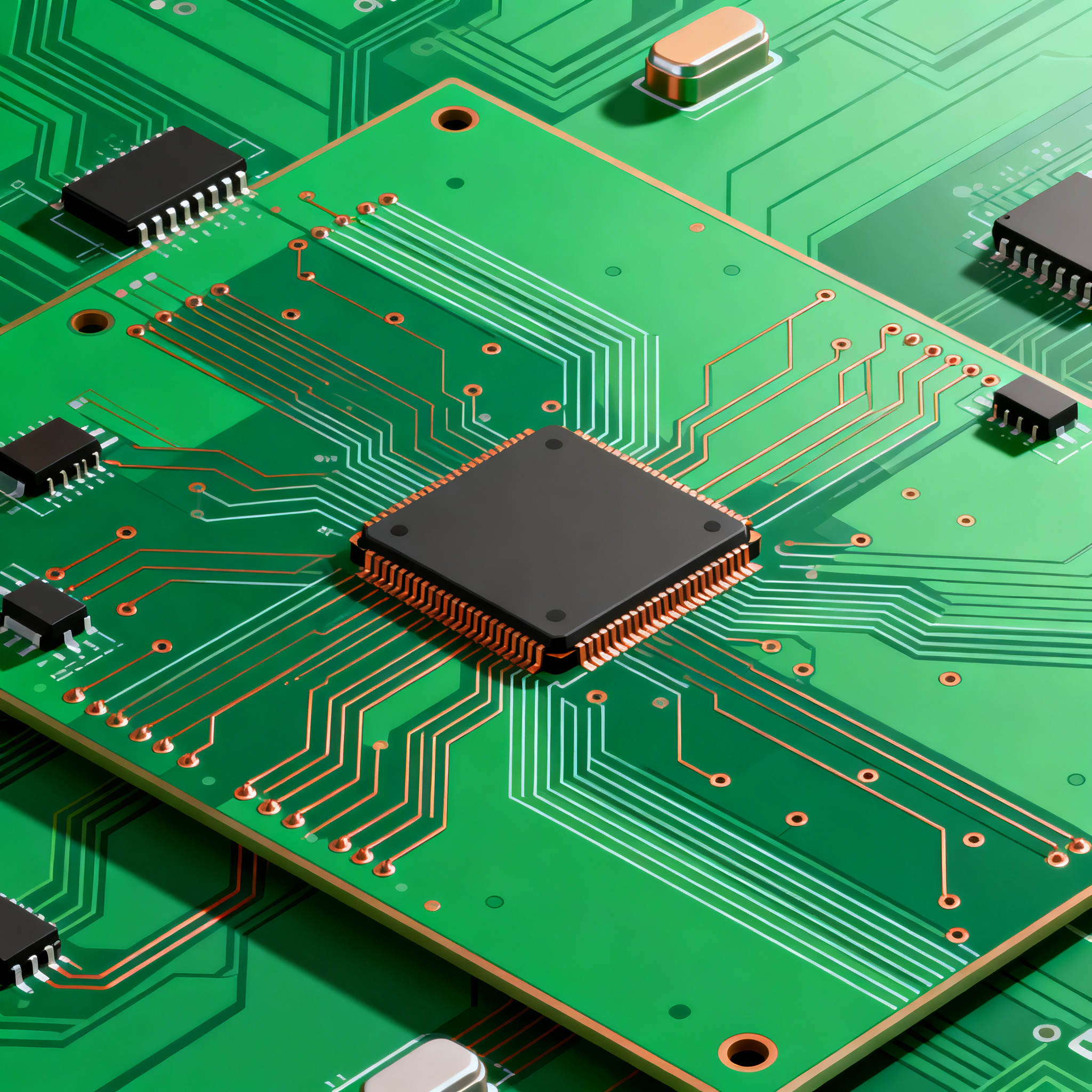
Mastering High-Speed PCB Design: Key Techniques for 4-Layer Boards
Mastering High-Speed PCB Design: Key Techniques for 4-Layer Boards Introduction In today's fast-paced electronics industry, high-speed PCB design has become a critical skill for engineers working with...
Introduction
In today's fast-paced electronics industry, high-speed PCB design has become a critical skill for engineers working with 4-layer boards. As devices grow more complex and performance demands increase, mastering these techniques is essential for ensuring reliable and efficient circuitry. This article delves into the intricacies of high-speed PCB design, focusing on circuit topology, component calculations, performance analysis, and design trade-offs. With the right approach, engineers can optimize board performance, minimize signal integrity issues, and meet stringent industry standards.
Technical Overview
High-speed PCB design involves managing signal integrity, power distribution, and thermal performance to achieve optimal circuit functionality. The core concepts include understanding the architecture of 4-layer boards, which typically consist of a signal layer, power plane, ground plane, and another signal layer. Proper layer stack-up is crucial for minimizing electromagnetic interference (EMI) and ensuring signal integrity. Engineers must consider factors like impedance control, trace width, and spacing, which are governed by IPC standards, such as IPC-2221 and IPC-A-610.
Another important aspect is the use of differential pairs and controlled impedance traces to minimize crosstalk and signal degradation. Components must be carefully selected and placed to reduce parasitic effects, and decoupling capacitors are vital for stable power delivery. Simulation tools and performance analysis are employed to predict and mitigate potential issues. Balancing these elements requires a thorough understanding of the trade-offs involved in high-speed PCB design.
Detailed Specifications
When designing high-speed PCBs, several specifications are critical to ensure optimal performance. These include trace impedance, layer stack-up, component placement, and routing strategies. Proper calculation and consideration of these parameters can significantly influence the board’s signal integrity and overall functionality.
| Design Parameter | Value/Formula | Explanation |
|---|---|---|
| Trace Impedance | 50 Ohms | Standard for digital signals to minimize reflections |
| Layer Stack-up | Signal-Ground-Power-Signal | Common 4-layer configuration for EMI reduction |
| Trace Width | 5 mils | Calculated for controlled impedance |
| Trace Spacing | 5 mils | Prevents crosstalk between adjacent traces |
| Via Size | 0.6 mm | Standard size for signal vias |
| Dielectric Constant (Er) | 4.2 | Material property impacting impedance and signal speed |
| Decoupling Capacitor | 0.1 µF | Used for power supply noise reduction |
| Power Plane Thickness | 1 oz copper | Ensures adequate current carrying capacity |
| Ground Plane Thickness | 1 oz copper | Provides a stable reference for signals |
| Signal Rise Time | 1 ns | Affects trace impedance and signal integrity |
Key Takeaways from the Specifications
The specifications outlined above are foundational to high-speed PCB design. Trace impedance of 50 Ohms is standard for digital signals, ensuring minimal signal reflections. The layer stack-up of Signal-Ground-Power-Signal is widely used to reduce electromagnetic interference and enhance signal integrity. Calculating trace width and spacing is crucial for maintaining controlled impedance and preventing crosstalk. Additionally, selecting appropriate via sizes and dielectric constants affects both the mechanical and electrical performance of the board. Understanding these parameters allows engineers to effectively design PCBs that meet performance and reliability requirements.
| Performance Metric | Value | Impact |
|---|---|---|
| Signal Gain | 10 dB | Determines the amplification level of the circuit |
| Bandwidth | 2 GHz | Frequency range over which the circuit operates effectively |
| Signal-to-Noise Ratio (SNR) | 60 dB | Indicates signal clarity and quality |
| Power Consumption | 2 W | Overall energy usage of the board |
| Thermal Resistance | 30 °C/W | Ability to dissipate heat |
| Latency | 5 ns | Time delay in signal processing |
| Crosstalk | -30 dB | Measures unwanted signal coupling between traces |
| Jitter | 10 ps | Variability in signal timing |
Practical Implications
The performance metrics provide insights into the operational capabilities of a high-speed PCB. Signal gain and bandwidth are critical for determining the circuit's effectiveness in amplifying and transmitting signals across frequencies. A high signal-to-noise ratio (SNR) ensures clarity, while power consumption indicates the board's efficiency. Thermal resistance is vital for heat management, preventing overheating and potential damage. Low latency and jitter are essential for maintaining signal timing accuracy, especially in high-speed applications. Understanding these metrics allows engineers to predict performance and make necessary adjustments during the design phase.
| Configuration | Pros | Cons |
|---|---|---|
| Standard 4-Layer | Cost-effective, simple design | Limited to moderate complexity circuits |
| Embedded Resistors | Reduces board space, improves performance | Increased manufacturing complexity |
| Microvias | Enables high-density interconnects | Higher cost, complex fabrication |
| Blind/Buried Vias | Increases routing density | Complicated design and manufacturing |
| High-Density Interconnect (HDI) | Supports advanced features, compact design | Expensive, requires precise manufacturing |
| Impedance Control | Ensures signal integrity | Requires meticulous design and testing |
| Thick Copper Layers | Improves current carrying capacity | Increases weight and cost |
Application Guidelines
When selecting a configuration for a high-speed PCB, engineers must weigh the pros and cons of each option. Standard 4-layer boards are suitable for cost-sensitive applications with moderate complexity. For high-performance needs, embedded resistors and microvias offer space-saving and performance benefits but at the expense of increased complexity and cost. High-density interconnects (HDI) are ideal for advanced features but require precise manufacturing processes. Impedance control is crucial for maintaining signal integrity, especially in high-speed designs. Engineers should choose configurations based on application requirements, cost constraints, and manufacturing capabilities.
Design Considerations
Designing a high-speed PCB involves numerous considerations to ensure optimal performance and reliability. Engineers must prioritize signal integrity, power distribution, and thermal management. Proper trace routing is essential to minimize reflections and crosstalk, often achieved through controlled impedance and differential pairs. Decoupling capacitors should be strategically placed near power pins to stabilize voltage levels and reduce noise.
Layer stack-up is another critical factor, with a common configuration being Signal-Ground-Power-Signal, which helps reduce EMI and improve signal integrity. Engineers must also consider the use of vias, as excessive use can introduce parasitic inductance and capacitance, impacting signal quality. Careful component selection and placement are essential to minimize parasitic effects and ensure efficient power distribution.
Thermal management is vital to prevent overheating and maintain board reliability. This can be addressed through adequate copper thickness, thermal vias, and heat sinks. Simulation tools are invaluable for predicting potential performance issues and optimizing the design before fabrication. By balancing these considerations, engineers can design high-speed PCBs that meet performance specifications and industry standards.
Step-by-Step Implementation
- Define the circuit requirements and performance goals, including signal integrity, power distribution, and thermal management.
- Select the appropriate layer stack-up, typically Signal-Ground-Power-Signal, to optimize EMI reduction and signal integrity.
- Calculate trace impedance and width to ensure controlled impedance and prevent reflections.
- Choose suitable components, such as decoupling capacitors, and place them strategically to stabilize voltage levels.
- Design trace routing with controlled impedance and differential pairs to minimize crosstalk and signal degradation.
- Implement thermal management strategies, such as using adequate copper thickness and thermal vias, to dissipate heat effectively.
- Utilize simulation tools to predict potential performance issues and refine the design accordingly.
- Conduct thorough testing and validation to ensure the PCB meets performance specifications and industry standards.
Common Issues & Solutions
- Signal Reflections: Often caused by impedance mismatches. Solution: Ensure controlled impedance through precise trace width calculations.
- Crosstalk: Unwanted signal coupling between traces. Solution: Increase trace spacing and use differential pairs.
- Power Supply Noise: Can lead to instability. Solution: Use decoupling capacitors near power pins.
- Thermal Overload: Excessive heat can damage components. Solution: Implement thermal vias and heat sinks.
- EMI Issues: Interference affecting signal integrity. Solution: Optimize layer stack-up and use ground planes.
- Manufacturing Defects: Can occur during fabrication. Solution: Follow IPC standards and conduct thorough inspections.
Applications & Use Cases
High-speed PCB design is crucial in various applications, from consumer electronics to telecommunications and automotive systems. In consumer electronics, these designs enable faster processing speeds and improved device performance. Telecommunications benefit from enhanced signal integrity and reduced latency, essential for reliable data transmission. In automotive systems, high-speed PCBs support advanced driver-assistance systems (ADAS) and infotainment features, requiring robust and reliable circuit performance.
Selection & Sourcing Guide
When sourcing components for high-speed PCB design, it's essential to choose reputable suppliers that offer quality and reliability. Consider using IC Online for a wide range of electronic components. Ensure that the components meet the required specifications and industry standards to guarantee optimal performance and compatibility with your PCB design.
FAQ
- What is the importance of controlled impedance in high-speed PCB design? Controlled impedance is crucial for minimizing signal reflections and ensuring signal integrity, especially in high-frequency applications.
- How can I reduce crosstalk in my PCB design? Increase trace spacing, use differential pairs, and implement proper layer stack-up to minimize crosstalk.
- What role do decoupling capacitors play in PCB design? They stabilize voltage levels and reduce power supply noise, ensuring stable circuit operation.
- Why is thermal management important in PCB design? Effective thermal management prevents overheating, ensuring component reliability and longevity.
- How do I choose the right layer stack-up? Consider EMI reduction, signal integrity, and power distribution needs when selecting a layer stack-up.
- What tools are available for simulating PCB performance? Simulation tools like SPICE and HFSS are commonly used for predicting and optimizing PCB performance.
- What are the common manufacturing challenges in high-speed PCB design? Challenges include maintaining controlled impedance, managing EMI, and ensuring precise fabrication.
- How do I ensure my PCB meets industry standards? Follow IPC standards and conduct thorough testing and validation to ensure compliance.
- What is the significance of using a ground plane? A ground plane provides a stable reference for signals, reducing EMI and improving signal integrity.
- Can I use standard vias in high-speed PCB design? While standard vias are commonly used, microvias and blind/buried vias offer advantages in high-density designs.
Conclusion
Mastering high-speed PCB design is essential for engineers working with 4-layer boards in today's electronics industry. By understanding the intricacies of circuit topology, component calculations, performance analysis, and design trade-offs, engineers can optimize board performance and meet stringent industry standards. With the right approach and tools, high-speed PCB design can enhance device performance, reliability, and functionality across various applications.