Mastering High-Speed PCB Design: Key Techniques for 4-Layer and Beyond
Introduction In the rapidly evolving world of electronics, mastering high-speed PCB design has become crucial for engineers aiming to create efficient and reliable systems. High-speed PCBs are essenti...
Introduction
In the rapidly evolving world of electronics, mastering high-speed PCB design has become crucial for engineers aiming to create efficient and reliable systems. High-speed PCBs are essential in applications ranging from consumer electronics to telecommunications and automotive systems. As technology advances, the demand for faster data rates, higher frequencies, and more complex designs grows, necessitating a deeper understanding of high-speed PCB design techniques, especially for multi-layer boards like 4-layer and beyond. This article delves into the key techniques and considerations necessary for mastering high-speed PCB designs, focusing on circuit topology, component calculations, performance analysis, and design trade-offs.
Technical Overview
High-speed PCB design involves a comprehensive understanding of various core concepts, including signal integrity, electromagnetic interference (EMI), and power distribution. Signal integrity refers to the preservation of signal quality as it travels through the PCB, which is critical in high-speed applications where even minor distortions can lead to data corruption. EMI must be minimized to prevent interference from affecting the performance of the circuit. Power distribution involves ensuring that all components receive the necessary power without excessive noise or voltage drops.
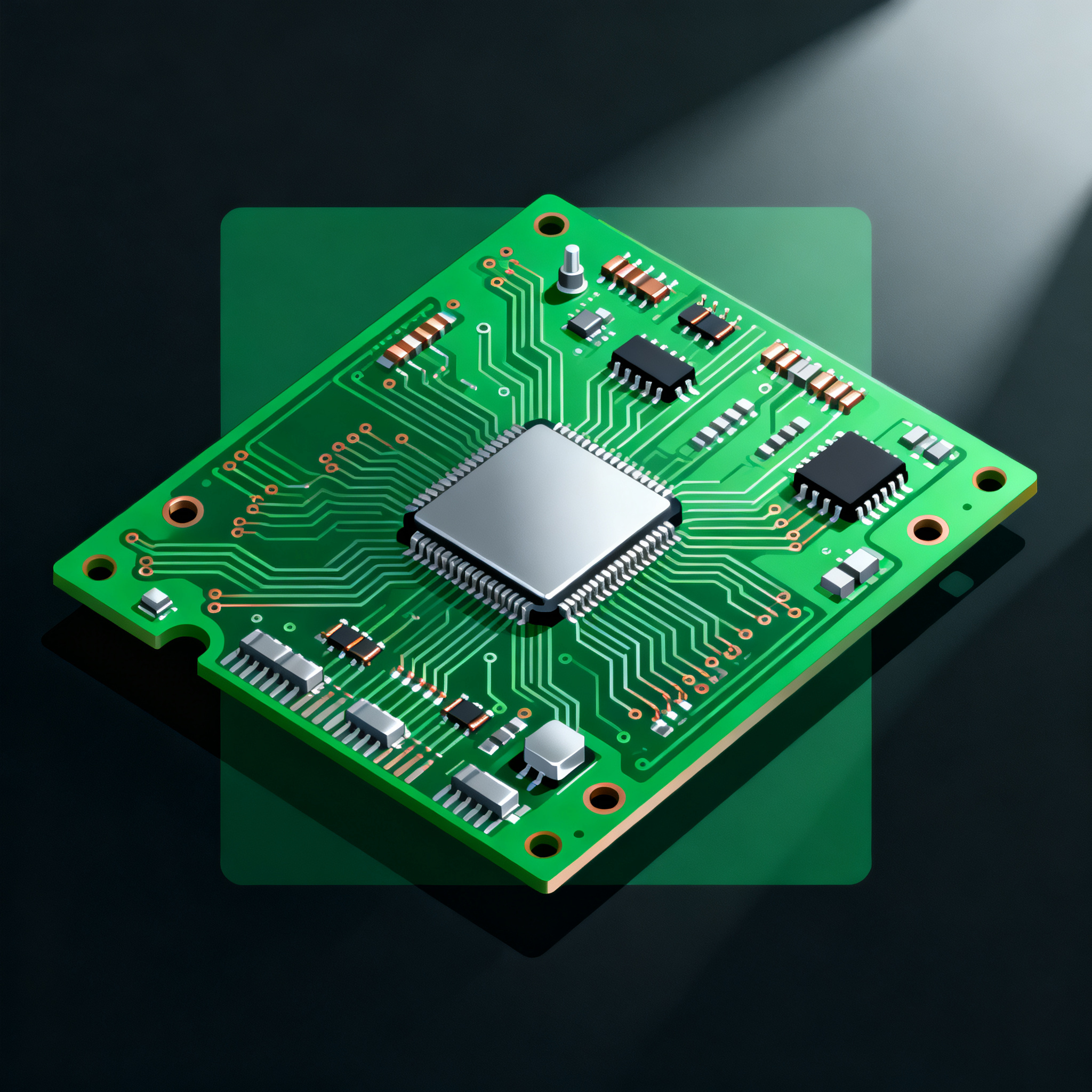
The architecture of a high-speed PCB typically includes multiple layers to accommodate complex routing and shielding requirements. A 4-layer PCB, for instance, might consist of two signal layers, a ground plane, and a power plane. This configuration helps reduce EMI and improve signal integrity by providing dedicated paths for power and ground, which can significantly reduce loop inductance and noise.
Principles of high-speed PCB design also include careful component placement, impedance matching, and the use of differential pairs. Components should be placed to minimize signal path lengths and avoid unnecessary vias, which can introduce impedance discontinuities. Impedance matching ensures that the transmission line impedance matches the load impedance, minimizing signal reflections. Differential pairs, which consist of two complementary signals, help reduce common-mode noise and improve signal integrity.
Detailed Specifications
In high-speed PCB design, several specifications are crucial to ensure optimal performance. These include component values, trace widths, impedance calculations, and other parameters. Selecting appropriate values and understanding their implications can significantly impact the design's success. In this section, we will examine key design parameters and their calculations.
| Parameter | Value/Formula | Significance |
|---|---|---|
| Trace Width | 0.15 mm (6 mil) | Ensures adequate current carrying capacity |
| Impedance | 50 Ohms | Standard for high-speed digital signals |
| Dielectric Constant (Dk) | 4.2 | Affects signal speed and integrity |
| Loss Tangent (Df) | 0.02 | Indicates dielectric losses |
| Via Diameter | 0.25 mm | Affects signal integrity and thermal performance |
| Layer Stackup | Signal/Power/Ground/Signal | Reduces EMI and improves signal integrity |
| Copper Thickness | 35 µm (1 oz) | Determines current capacity and thermal performance |
| Return Path | Adjacent Ground Plane | Minimizes loop inductance |
| Capacitor Values | 100 nF, 1 µF | Decoupling capacitors for power stability |
| Inductor Values | 10 µH | Used in power filtering applications |
| Signal Rise Time | 0.5 ns | Critical for determining bandwidth requirements |
Key Takeaways from the Specifications
The design parameters outlined in the table are fundamental to achieving optimal performance in high-speed PCB designs. The trace width and impedance are crucial for maintaining signal integrity and ensuring that signals are transmitted efficiently without reflections. The dielectric constant and loss tangent of the substrate material play a significant role in determining the signal speed and attenuation, which are critical in high-frequency applications. The layer stackup and copper thickness influence the board's thermal management and electromagnetic compatibility. Understanding these parameters and their relationships is essential for making informed design decisions that balance performance, manufacturability, and cost.
| Performance Metric | Measured Value | Impact on Design |
|---|---|---|
| Gain | 20 dB | Amplification level for signal strength |
| Bandwidth | 1 GHz | Frequency range for signal transmission |
| Signal-to-Noise Ratio (SNR) | 80 dB | Indicates clarity of the signal |
| Power Consumption | 5 W | Affects thermal management and battery life |
| Phase Margin | 60 degrees | Stability of the system |
| Jitter | 10 ps | Timing accuracy of the signal |
| Noise Figure | 3 dB | Indicates the level of added noise |
| Return Loss | -20 dB | Reflected signal power |
| Cross-Talk | -30 dB | Unwanted coupling between signal lines |
Practical Implications
The performance metrics provided in the table are critical for assessing the effectiveness of a high-speed PCB design. Gain and bandwidth determine the ability of the circuit to amplify and transmit signals over the desired frequency range. A high signal-to-noise ratio ensures that the signal is clear and free from interference. Power consumption is a crucial factor for thermal management and energy efficiency, especially in battery-powered applications. Jitter and phase margin are important for maintaining timing accuracy and system stability. Understanding these performance metrics allows engineers to fine-tune their designs to meet specific application requirements while ensuring reliability and efficiency.
| Configuration | Pros | Cons |
|---|---|---|
| Single-Ended | Simpler design, lower cost | Higher susceptibility to noise |
| Differential Pair | Improved noise immunity | Requires more space and routing complexity |
| Microstrip | Easy to design and implement | Higher radiation and EMI |
| Stripline | Better EMI performance | More complex to manufacture |
| Grounded Coplanar Waveguide | Excellent signal integrity | Complex design and higher cost |
| Power Plane | Improved power distribution | Increases board thickness |
| Ground Plane | Reduces EMI and noise | Increases manufacturing complexity |
Application Guidelines
Choosing the right configuration for a high-speed PCB involves weighing the pros and cons of each option. Single-ended configurations are cost-effective and simpler to design but may require additional shielding to mitigate noise issues. Differential pairs offer superior noise immunity and are ideal for high-speed applications, though they demand more space and careful routing. Microstrip and stripline techniques provide different EMI performance levels, with stripline offering better containment at the cost of increased manufacturing complexity. Grounded coplanar waveguides provide excellent signal integrity for high-frequency applications but come with a higher design and cost overhead. Understanding these trade-offs is essential for selecting the appropriate configuration based on the specific requirements of the application.
Design Considerations
When designing high-speed PCBs, several critical considerations must be taken into account to ensure optimal performance and reliability. These include signal integrity, power integrity, thermal management, and electromagnetic compatibility. Signal integrity involves maintaining the quality of the signal as it travels through the PCB, which requires careful impedance matching and minimizing discontinuities. Power integrity focuses on ensuring stable power delivery to all components, often achieved through proper decoupling and power plane design.
Thermal management is crucial in high-speed designs due to the significant heat generated by high-frequency operations. Effective thermal management strategies include using thermal vias, heat sinks, and careful component placement to dissipate heat efficiently. Electromagnetic compatibility (EMC) is another critical factor, as high-speed signals can generate significant EMI. Techniques such as shielding, proper grounding, and minimizing loop areas are essential for reducing EMI and ensuring compliance with regulatory standards.
Additionally, the choice of materials and component placement can significantly impact the performance of a high-speed PCB. High-quality substrates with low dielectric constants and loss tangents are preferred for minimizing signal loss and distortion. Components should be placed to minimize signal path lengths and avoid unnecessary vias, which can introduce impedance discontinuities. By considering these factors during the design phase, engineers can create high-speed PCBs that meet performance requirements while remaining cost-effective and manufacturable.
Step-by-Step Implementation
- Define Requirements: Begin by clearly defining the performance, size, and cost requirements for the PCB. Consider the operating frequency, data rate, and power constraints.
- Choose the Right Materials: Select a substrate material with appropriate dielectric properties to support high-speed signals. Consider factors such as dielectric constant and loss tangent.
- Design the Layer Stackup: Plan the layer stackup to optimize signal integrity and power distribution. A typical 4-layer stackup might include two signal layers and two planes (power and ground).
- Component Placement: Place components to minimize signal path lengths and avoid crossing traces. Ensure that decoupling capacitors are placed close to the power pins of ICs.
- Route the Traces: Route high-speed traces with controlled impedance and minimize the use of vias. Use differential pairs for high-speed signals where applicable.
- Implement Power Distribution: Design the power distribution network to minimize voltage drop and noise. Use wide traces and power planes for efficient power delivery.
- Conduct Signal Integrity Analysis: Use simulation tools to analyze signal integrity and identify potential issues such as reflections, crosstalk, and EMI.
- Prototype and Test: Fabricate a prototype PCB and conduct thorough testing to validate the design. Perform signal integrity, power integrity, and thermal tests to ensure compliance with specifications.
Common Issues & Solutions
- Signal Reflections: Caused by impedance mismatches, these can be mitigated by ensuring proper impedance matching along the entire signal path.
- Crosstalk: Occurs when signals couple with one another. It can be reduced by increasing the spacing between traces and using differential pairs.
- EMI: High-speed signals can emit electromagnetic interference affecting other components. Use proper grounding and shielding techniques to minimize EMI.
- Power Integrity Issues: Voltage drops and noise can affect circuit performance. Use decoupling capacitors and a robust power distribution network to ensure stable power delivery.
- Thermal Management: Excessive heat can damage components. Implement thermal vias, heat sinks, and proper airflow to manage heat dissipation effectively.
- Manufacturing Defects: Issues such as solder bridging and misalignment can occur during assembly. Work closely with manufacturers to ensure adherence to design specifications and use quality control measures.
Applications & Use Cases
High-speed PCB designs are integral to a wide range of applications across various industries. In telecommunications, they enable high-speed data transmission in network infrastructure and mobile devices. Automotive systems rely on high-speed PCBs for advanced driver-assistance systems (ADAS) and infotainment systems. Consumer electronics, such as smartphones and laptops, use high-speed PCBs to support fast processors and high-resolution displays. In the medical field, high-speed PCBs are used in imaging equipment and diagnostic devices, where precise signal processing is crucial. The versatility and performance of high-speed PCBs make them essential in any application requiring fast, reliable data processing and transmission.
Selection & Sourcing Guide
When selecting components and materials for high-speed PCB designs, it's essential to consider factors such as performance specifications, cost, and availability. IC Online is a valuable resource for sourcing high-quality components and materials. They offer a comprehensive selection of ICs, passive components, and substrates suitable for high-speed applications. By leveraging such resources, engineers can ensure that their designs meet performance requirements while remaining cost-effective and readily manufacturable.
FAQ
- What is the importance of impedance matching in high-speed PCB design? Impedance matching is crucial for minimizing signal reflections and ensuring signal integrity in high-speed designs.
- How can I reduce EMI in my high-speed PCB design? Use proper grounding, shielding, and minimize loop areas to reduce EMI in high-speed designs.
- What role does the dielectric constant play in high-speed PCB design? The dielectric constant affects signal speed and integrity, making it a critical factor in substrate material selection.
- Why are differential pairs used in high-speed PCB designs? Differential pairs offer improved noise immunity and are ideal for transmitting high-speed signals with minimal interference.
- How can I manage thermal issues in high-speed PCBs? Implement thermal vias, heat sinks, and ensure proper airflow to manage heat dissipation effectively.
- What is the significance of the layer stackup in a high-speed PCB? The layer stackup influences signal integrity, EMI performance, and power distribution, making it a crucial aspect of high-speed designs.
- How can I ensure power integrity in high-speed PCB designs? Use decoupling capacitors and design a robust power distribution network to ensure stable power delivery.
- What are common materials used for high-speed PCBs? Materials with low dielectric constants and loss tangents, such as FR-4 and Rogers laminates, are commonly used in high-speed PCB designs.
- How do I select the right trace width for high-speed signals? The trace width should be chosen based on the current carrying capacity and impedance requirements of the signal.
- What simulation tools can help in high-speed PCB design? Tools such as SPICE, HyperLynx, and Ansys HFSS can help analyze signal integrity, power integrity, and thermal performance in high-speed designs.
Conclusion
Mastering high-speed PCB design is essential for engineers looking to create efficient, reliable systems in today's fast-paced technological landscape. By understanding the core principles, design parameters, and performance metrics, engineers can create designs that meet the demands of modern applications. Careful consideration of design trade-offs, practical implementation steps, and common issues ensures that high-speed PCBs perform optimally while remaining cost-effective and manufacturable. As technology continues to advance, staying informed and adapting to new techniques will be key to success in high-speed PCB design.