Mastering High-Speed PCB Design: Essential Techniques for 4-Layer Boards
Mastering High-Speed PCB Design: Essential Techniques for 4-Layer Boards body { font-family: Arial, sans-serif; line-height: 1.6; margin: 20px; } h2 { color: #333; } table { border-collapse: collapse;...
Introduction
In today's fast-paced world of electronics, the demand for high-speed and reliable printed circuit boards (PCBs) is ever-increasing. As devices become more sophisticated and interconnected, the need for efficient and effective PCB design becomes paramount. High-speed PCB design, particularly for 4-layer boards, is crucial for ensuring signal integrity, reducing electromagnetic interference, and optimizing performance. This guide offers essential techniques and insights into mastering high-speed PCB design, focusing on circuit topology, component calculations, performance analysis, and design trade-offs.
Technical Overview
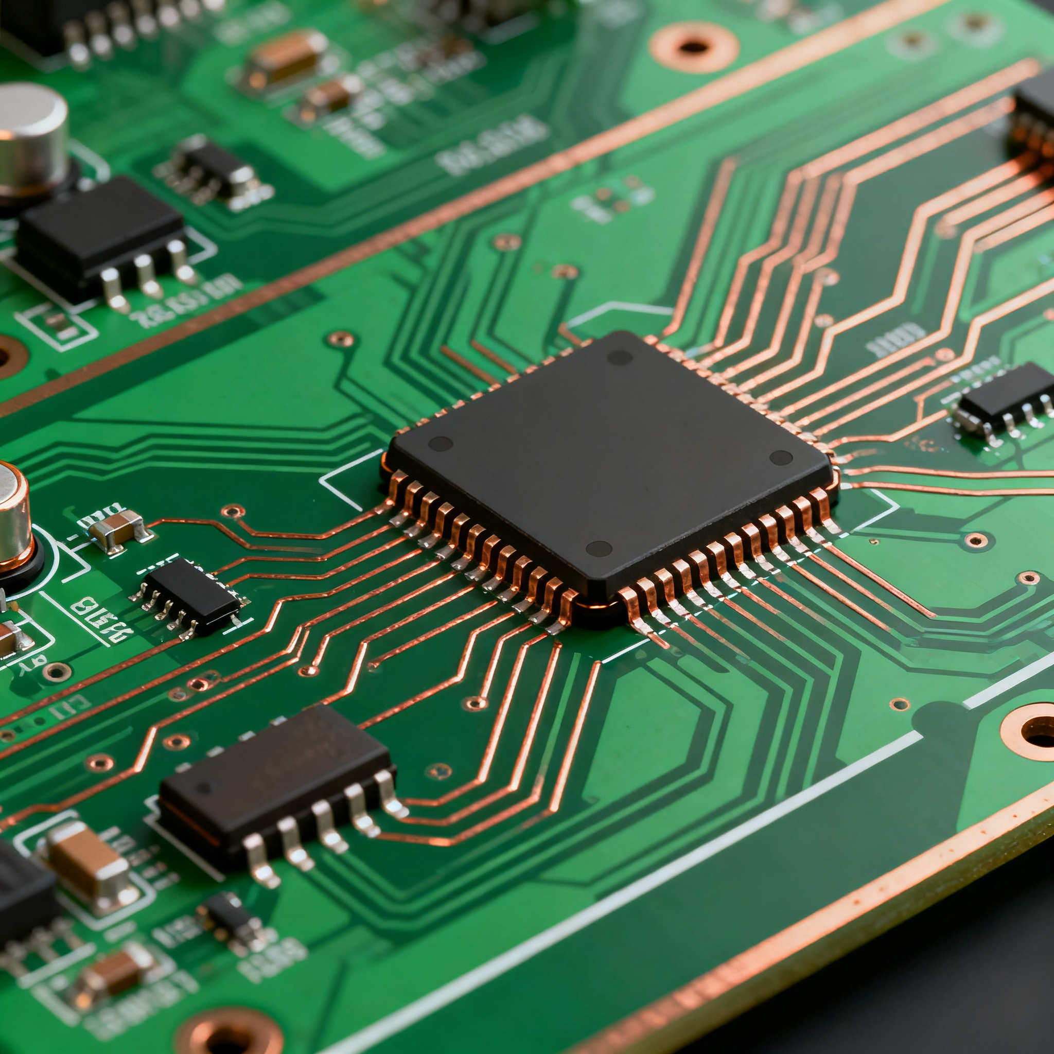
High-speed PCB design involves the careful consideration of various technical factors that influence the performance and reliability of electronic circuits. Core concepts include understanding the architecture of 4-layer boards, the principles of signal integrity, and the impact of electromagnetic interference. The architecture of 4-layer boards typically consists of a signal layer, a ground plane, a power plane, and another signal layer. This configuration helps in minimizing cross-talk and ensuring a stable power distribution network. Key principles such as controlled impedance, differential signaling, and proper termination techniques are vital for maintaining signal integrity at high frequencies.
Moreover, understanding the role of bypass capacitors, decoupling strategies, and the placement of components significantly impacts the overall design. The choice of materials, such as low-loss dielectrics, and the implementation of effective grounding techniques also play a critical role in high-speed PCB design. By adhering to industry standards such as IPC-2221 and IPC-A-610, designers can ensure compliance with quality and performance benchmarks.
Detailed Specifications
When designing high-speed PCBs, several specifications must be considered to ensure optimal performance. These specifications include component values, trace widths, impedance control, and power distribution network design. Accurate calculations and adherence to design rules are essential in achieving the desired electrical characteristics and avoiding potential design pitfalls.
| Parameter | Value/Formula | Description |
|---|---|---|
| Trace Width | 0.2mm | Width of the PCB trace to control impedance |
| Dielectric Constant (εr) | 4.5 | Material property affecting signal speed and impedance |
| Impedance (Z0) | 50Ω | Characteristic impedance for signal integrity |
| Bypass Capacitor | 0.1µF | For power supply noise reduction |
| Via Diameter | 0.3mm | Size of vias used for layer transitions |
| Layer Stack-up | Signal-Ground-Power-Signal | Layer configuration for optimal performance |
| Trace Length | ≤ 100mm | Maximum length to prevent signal degradation |
| Return Path | Directly beneath signal trace | Ensures minimal loop area for signal return |
| Power Plane Thickness | 1oz copper | Thickness for adequate current carrying capability |
| Signal Rise Time | ≤ 1ns | Maximum rise time for signal integrity |
Key Takeaways from the Specifications
The detailed specifications listed in Table 1 highlight critical parameters necessary for high-speed PCB design. The trace width and dielectric constant play a pivotal role in controlling the impedance, which is essential for maintaining signal integrity. A characteristic impedance of 50Ω is typically targeted to match transmission line requirements. The use of bypass capacitors is crucial for reducing power supply noise, while the specific layer stack-up ensures optimal signal routing and power distribution. Proper via size and placement are necessary to facilitate efficient layer transitions without introducing excessive inductance. Adhering to these specifications helps in minimizing signal degradation and electromagnetic interference.
| Performance Metric | Value | Remarks |
|---|---|---|
| Gain | 10dB | Amplification factor of the circuit |
| Bandwidth | 2GHz | Frequency range over which the circuit operates effectively |
| Noise Figure | 3dB | Measure of noise introduced by the circuit |
| Power Consumption | 5W | Total power used by the circuit |
| Signal-to-Noise Ratio (SNR) | 50dB | Ratio of signal power to noise power |
| Return Loss | 20dB | Measure of signal reflection at the input |
| Insertion Loss | 0.5dB | Loss of signal power resulting from insertion into the circuit |
| Phase Margin | 60° | Stability measure of the circuit |
Practical Implications
Table 2 presents critical performance metrics that influence the effectiveness of high-speed PCB designs. The gain and bandwidth determine the amplification capabilities and the frequency range of operation, respectively. A noise figure of 3dB indicates the level of noise introduced by the circuit, impacting overall performance. Power consumption is a crucial consideration for thermal management and efficiency. A high signal-to-noise ratio ensures clear signal transmission, while return and insertion losses affect signal integrity. The phase margin is essential for ensuring circuit stability, preventing oscillations and ensuring reliable operation.
| Configuration | Pros | Cons |
|---|---|---|
| Microstrip Line | Easy to design and fabricate | Higher radiation loss |
| Stripline | Low radiation loss | Complex fabrication |
| Grounded Coplanar Waveguide | Good isolation | Increased complexity |
| Embedded Resistors | Space-saving | Higher cost |
| Thick Copper Layers | High current carrying capability | Increased cost and weight |
| Blind/Buried Vias | Reduced board size | Complex manufacturing |
| Surface Mount Technology (SMT) | Higher component density | Requires precise placement |
Application Guidelines
The design trade-offs outlined in Table 3 highlight the advantages and disadvantages of various PCB configurations. Microstrip lines offer simplicity but at the cost of increased radiation loss, while striplines provide low radiation loss but require more complex fabrication processes. Grounded coplanar waveguides offer excellent isolation but add complexity to the design. Embedded resistors save space but come with a higher cost. Thick copper layers enhance current carrying capability but increase both cost and weight. Blind and buried vias reduce board size but complicate manufacturing. Surface mount technology allows for higher component density but demands precise placement. Careful consideration of these trade-offs is essential for optimizing PCB design.
Design Considerations
Designing a high-speed PCB involves balancing multiple factors to ensure optimal performance and reliability. Key considerations include signal integrity, power integrity, thermal management, and electromagnetic compatibility. Signal integrity is maintained by controlling impedance, minimizing cross-talk, and ensuring proper termination. Power integrity involves designing an efficient power distribution network with adequate decoupling and bypass capacitors. Thermal management is crucial for preventing overheating and ensuring long-term reliability. Techniques such as heat sinks, thermal vias, and proper component placement play a vital role in thermal management.
Electromagnetic compatibility is achieved by minimizing electromagnetic emissions and susceptibility through careful layout and grounding strategies. The choice of materials, such as low-loss dielectrics and high-frequency laminates, also impacts the overall performance of the PCB. Additionally, adhering to industry standards and guidelines, such as those outlined by IPC and other regulatory bodies, ensures compliance and quality assurance. By considering these factors, designers can create high-speed PCBs that meet the demanding requirements of modern electronic devices.
Step-by-Step Implementation
- Define Requirements: Clearly outline the performance and functional requirements of the PCB.
- Schematic Design: Create a detailed schematic diagram that includes all components and their connections.
- Component Selection: Choose components based on performance, availability, and cost considerations.
- Layout Design: Design the PCB layout, ensuring proper component placement and routing.
- Impedance Control: Calculate and adjust trace widths to achieve the desired impedance.
- Power Distribution Network: Design an efficient power distribution network with adequate decoupling.
- Thermal Management: Implement thermal management strategies to prevent overheating.
- Design Review and Verification: Conduct a thorough design review and verification process to ensure all requirements are met.
Common Issues & Solutions
- Signal Integrity Issues: Use controlled impedance and proper termination techniques to prevent signal degradation.
- Power Integrity Problems: Implement adequate decoupling and bypass capacitors to reduce power supply noise.
- Thermal Management Challenges: Use heat sinks and thermal vias to manage heat dissipation effectively.
- Electromagnetic Interference (EMI): Employ proper grounding and shielding techniques to minimize EMI.
- Component Placement Errors: Ensure components are placed to minimize trace lengths and cross-talk.
- Manufacturing Defects: Adhere to design for manufacturability (DFM) guidelines to reduce defects.
Applications & Use Cases
High-speed PCBs are used in a wide range of applications, including telecommunications, data centers, automotive systems, and consumer electronics. In telecommunications, high-speed PCBs are essential for supporting high data rates and ensuring reliable signal transmission. Data centers rely on high-speed PCBs for efficient data processing and communication. In automotive systems, high-speed PCBs enable advanced driver-assistance systems (ADAS) and infotainment systems. Consumer electronics, such as smartphones and tablets, use high-speed PCBs to support high-performance processors and wireless communication.
Selection & Sourcing Guide
When selecting and sourcing components for high-speed PCB design, it is essential to consider factors such as performance, availability, and cost. Online resources such as IC Online provide a comprehensive database of electronic components, allowing designers to compare specifications and prices. Additionally, working with reputable PCB manufacturers and assembly services, such as PCBWay and Nova PCBA, ensures high-quality fabrication and assembly, meeting the demands of modern electronic devices.
FAQ
- What is the importance of impedance control in high-speed PCB design? Impedance control is crucial for maintaining signal integrity and preventing signal reflections, which can degrade performance.
- How can I reduce electromagnetic interference in my PCB design? Use proper grounding, shielding, and layout techniques to minimize electromagnetic emissions and susceptibility.
- What role do bypass capacitors play in PCB design? Bypass capacitors help reduce power supply noise and stabilize voltage levels, improving power integrity.
- Why is thermal management important in PCB design? Effective thermal management prevents overheating and ensures the long-term reliability of electronic components.
- What are the common challenges in high-speed PCB design? Common challenges include maintaining signal integrity, managing power distribution, and ensuring thermal performance.
- How do I choose the right materials for my PCB? Consider factors such as dielectric constant, loss tangent, and thermal properties when selecting materials for high-speed PCBs.
- What are the benefits of using a 4-layer PCB? A 4-layer PCB provides improved signal integrity, reduced electromagnetic interference, and efficient power distribution.
- How can I ensure my PCB design meets industry standards? Adhere to IPC standards and guidelines, and conduct thorough design reviews and testing to ensure compliance.
- What is the significance of signal rise time in PCB design? Signal rise time affects the bandwidth and signal integrity, and should be minimized for high-speed applications.
- How do I handle design trade-offs in PCB design? Carefully evaluate the pros and cons of different configurations to optimize performance and cost-effectiveness.
Conclusion
Mastering high-speed PCB design for 4-layer boards requires a comprehensive understanding of technical principles, detailed specifications, and design trade-offs. By focusing on signal integrity, power integrity, thermal management, and electromagnetic compatibility, designers can create reliable and efficient PCBs that meet the demands of modern electronic applications. Adhering to industry standards and leveraging advanced design techniques ensures high-performance PCBs that support the ever-evolving landscape of electronics.