Mastering 4-Layer PCB Stack-Up Optimization for Enhanced Signal Integrity
Mastering 4-Layer PCB Stack-Up Optimization for Enhanced Signal Integrity table { border-collapse: collapse; width: 100%; margin: 20px 0; } th, td { border: 1px solid #ddd; padding: 8px; } th { backgr...
Introduction
In the fast-evolving electronics industry, optimizing printed circuit board (PCB) design is crucial for achieving superior performance and reliability. A 4-layer PCB stack-up is a popular choice due to its balance between complexity, cost, and functionality. Mastering stack-up optimization can significantly enhance signal integrity, reduce electromagnetic interference, and improve overall device performance. This article delves into the intricacies of 4-layer PCB stack-up optimization, focusing on layout rules, stackup design, signal integrity, and manufacturing considerations.
Technical Overview
PCB stack-up design is a fundamental aspect of modern electronics, influencing signal integrity and electromagnetic compatibility (EMC). A typical 4-layer PCB consists of two signal layers and two planes for power and ground. This configuration helps in minimizing signal crosstalk and impedance mismatches, which are critical for high-speed applications. Understanding the principles of capacitance, inductance, and impedance is essential for optimizing the stack-up. The balance between trace width, spacing, and layer arrangement can mitigate issues related to signal degradation and electromagnetic interference (EMI).
Detailed Specifications
Design specifications are the cornerstone of any successful PCB project. They dictate the rules and guidelines for trace width, spacing, via sizes, and clearances, ensuring that the PCB meets its performance criteria. Adhering to these specifications minimizes errors during manufacturing and enhances the board's reliability. Below is a table outlining typical PCB design rules.
| Parameter | Minimum Value | Recommended Value |
|---|---|---|
| Trace Width | 4 mils | 6 mils |
| Trace Spacing | 4 mils | 8 mils |
| Via Hole Size | 0.2 mm | 0.3 mm |
| Via Pad Size | 0.4 mm | 0.6 mm |
| Clearance to Edge | 0.5 mm | 1.0 mm |
| Power Plane Clearance | 0.25 mm | 0.5 mm |
| Ground Plane Clearance | 0.25 mm | 0.5 mm |
| Solder Mask Clearance | 3 mils | 5 mils |
| Silkscreen Clearance | 4 mils | 6 mils |
| Minimum Annular Ring | 0.1 mm | 0.2 mm |
Key Takeaways from the Specifications
The table above highlights critical design parameters that ensure the functionality and manufacturability of a PCB. Trace width and spacing are crucial for controlling impedance and reducing crosstalk, especially in high-frequency circuits. Via sizes and clearances are important for ensuring reliable connections and preventing short circuits. Adhering to recommended values enhances the board's performance and reduces the risk of manufacturing defects. These specifications serve as a blueprint for achieving optimal signal integrity and reliability in PCB designs.
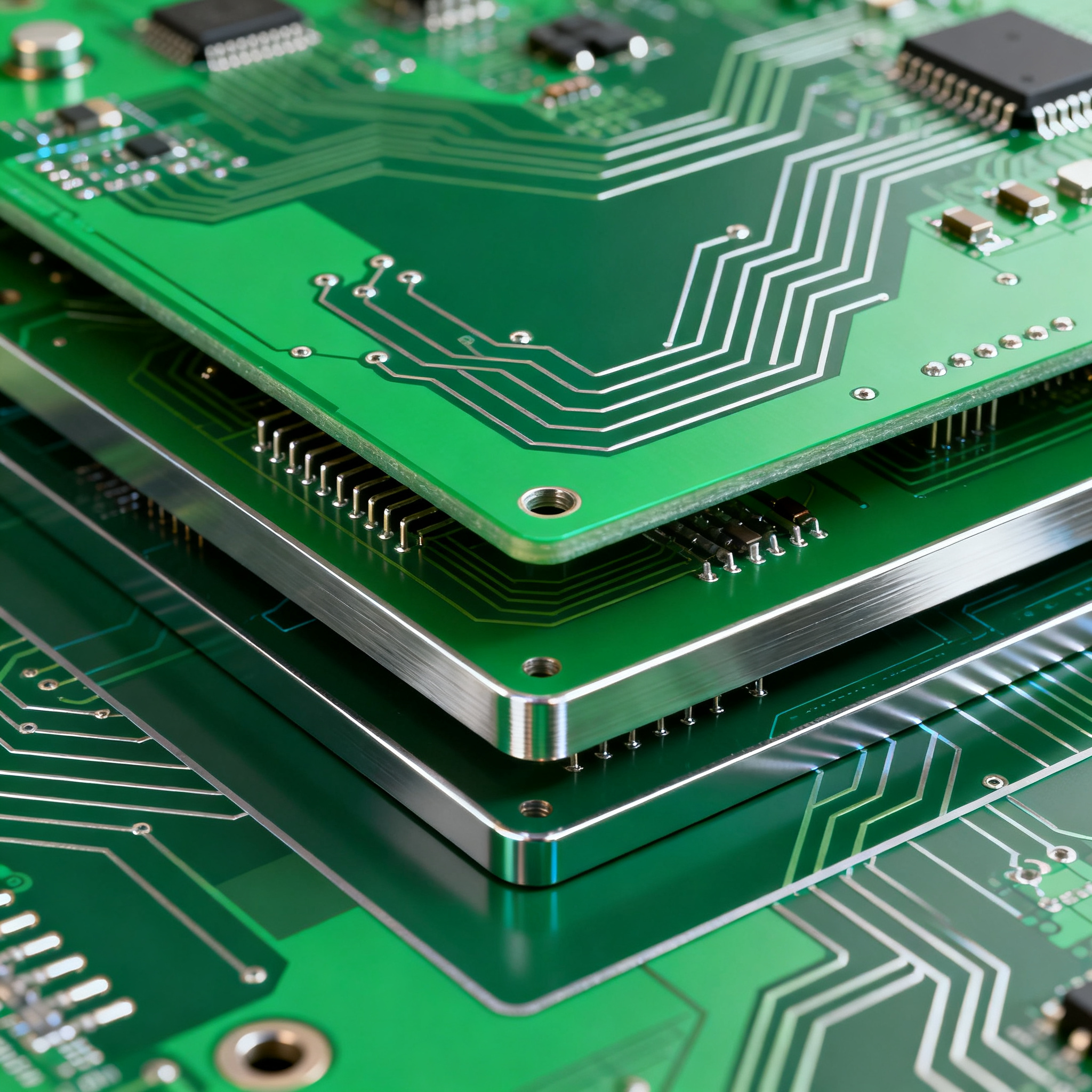
Layer Stackup Options
The layer stack-up is a strategic arrangement of conductive and insulating layers within a PCB. It plays a vital role in electromagnetic compatibility and signal integrity. Below is a table showing various 4-layer stack-up configurations commonly used in PCB design.
| Configuration | Layer 1 | Layer 4 |
|---|---|---|
| Standard | Signal | Signal |
| Power-Ground Sandwich | Signal | Signal |
| Ground-Power Sandwich | Ground | Power |
| Signal-Power-Ground-Signal | Signal | Signal |
| Ground-Signal-Power-Signal | Ground | Signal |
| Signal-Ground-Power-Signal | Signal | Signal |
Practical Implications
The stack-up configurations listed in the table are tailored to different application needs. A standard configuration is suitable for general-purpose applications, while a power-ground sandwich offers improved power distribution and signal integrity. Ground-signal-power-signal arrangements are ideal for minimizing EMI and improving high-frequency performance. Selecting the appropriate stack-up depends on the specific requirements of the application, including impedance control, EMI mitigation, and thermal management. Understanding these configurations aids in designing a PCB that meets both electrical and mechanical constraints.
Material Properties
The choice of materials significantly impacts the electrical performance and manufacturing costs of a PCB. Dielectric constants and loss tangents are critical factors in material selection. The table below provides an overview of common materials used in PCB manufacturing and their properties.
| Material | Dielectric Constant | Loss Tangent |
|---|---|---|
| FR-4 | 4.2-4.7 | 0.02 |
| Rogers 4350B | 3.48 | 0.0037 |
| Rogers 4003C | 3.55 | 0.0027 |
| Isola FR408HR | 3.7 | 0.009 |
| Nelco N4000-13 | 3.7 | 0.009 |
| Panasonic Megtron 6 | 3.5 | 0.002 |
| Arlon 85N | 3.5 | 0.003 |
| Polyimide | 3.5-4.0 | 0.004 |
Application Guidelines
The selection of PCB materials is a critical decision that affects signal integrity and thermal performance. FR-4 is a versatile and cost-effective material suitable for most applications, while Rogers materials are preferred for high-frequency designs due to their low loss tangent. The dielectric constant influences the propagation speed of signals, and lower values are generally better for high-speed circuits. Understanding these material properties helps designers make informed choices that align with their performance requirements and budget constraints.
Design Considerations
When designing a 4-layer PCB stack-up, several factors must be considered to ensure optimal performance and manufacturability. Firstly, trace impedance must be controlled to prevent signal reflection and degradation. This can be achieved by carefully selecting trace widths and spacing, as well as the dielectric materials used. Additionally, power integrity is crucial, requiring proper decoupling and power distribution strategies to minimize voltage fluctuations.
Thermal management is another key consideration, as heat dissipation can affect both performance and reliability. Thermal vias and heat sinks should be incorporated where necessary to maintain safe operating temperatures. Furthermore, the placement of components and routing of traces should be optimized to reduce crosstalk and electromagnetic interference. This involves maintaining adequate clearance between traces and ensuring that critical signals are isolated from noisy environments.
Finally, manufacturing constraints must be taken into account. This includes adhering to the PCB fabricator's capabilities in terms of minimum trace widths, spacing, and via sizes. By considering these design aspects from the outset, engineers can create robust and reliable PCBs that meet both electrical and mechanical requirements.
Step-by-Step Implementation
- Define Design Requirements: Establish the electrical and mechanical specifications for the PCB, including signal integrity, power distribution, thermal management, and EMI requirements.
- Select Materials: Choose appropriate dielectric materials based on the application's frequency and thermal requirements, balancing performance and cost.
- Plan Layer Stack-Up: Determine the optimal layer configuration for signal, power, and ground planes, considering impedance control and EMI mitigation.
- Design Schematic: Create a detailed circuit schematic, defining all electrical connections, components, and signal paths.
- Layout PCB: Use PCB design software to arrange components, route traces, and define vias, ensuring compliance with design rules and specifications.
- Perform Signal Integrity Analysis: Simulate the PCB design to verify signal integrity, impedance control, and crosstalk levels, making adjustments as needed.
- Review Design for Manufacturability: Ensure the design adheres to the PCB fabricator's capabilities, including minimum trace widths, spacing, and via sizes.
- Finalize Design and Documentation: Prepare the final design files, including Gerber files, Bill of Materials (BOM), and assembly drawings, for manufacturing and assembly.
Common Issues & Solutions
- Impedance Mismatch: Use controlled impedance traces and match trace widths to the characteristic impedance of the transmission line.
- Signal Crosstalk: Increase trace spacing and use ground planes to isolate high-speed signals.
- Electromagnetic Interference (EMI): Implement proper grounding and shielding techniques, and use decoupling capacitors to minimize EMI.
- Thermal Management: Incorporate thermal vias and heat sinks, and use materials with high thermal conductivity.
- Manufacturing Defects: Ensure the design complies with the fabricator's capabilities and perform thorough design rule checks.
- Power Integrity Issues: Use a solid power plane and adequate decoupling capacitors to stabilize power distribution.
Applications & Use Cases
4-layer PCBs are widely used in various applications, including consumer electronics, automotive systems, industrial equipment, and telecommunications. In consumer electronics, they provide the necessary signal integrity and power distribution for complex devices like smartphones and laptops. In automotive systems, 4-layer PCBs are used in engine control units and infotainment systems, where reliability and performance are critical. Industrial equipment benefits from the enhanced EMI performance and thermal management provided by 4-layer PCBs, while telecommunications applications leverage their ability to support high-frequency signals and data rates.
Selection & Sourcing Guide
When selecting and sourcing components for a 4-layer PCB, it is essential to consider the specific requirements of the application and the capabilities of the suppliers. Utilize online resources such as IC Online to find reliable suppliers and compare component specifications and prices. Ensure that the selected components meet the performance, quality, and cost criteria for your project.
FAQ
- What is the advantage of a 4-layer PCB over a 2-layer PCB? The additional layers in a 4-layer PCB allow for improved signal integrity, better power distribution, and enhanced EMI performance, making them suitable for more complex and high-speed applications.
- How do I choose the right stack-up for my PCB design? Consider the application's requirements for signal integrity, power distribution, and EMI control. Choose a stack-up that provides the necessary performance while adhering to manufacturing constraints.
- What materials are best for high-frequency PCB designs? Materials with low dielectric constants and loss tangents, such as Rogers 4350B and Panasonic Megtron 6, are ideal for high-frequency applications.
- How can I control impedance in my PCB design? Use controlled impedance traces by selecting appropriate trace widths and spacing, and ensure a consistent dielectric thickness between layers.
- What are the common causes of signal crosstalk? Signal crosstalk is often caused by inadequate spacing between traces and insufficient isolation from ground planes.
- How can I improve thermal management in my PCB design? Incorporate thermal vias, heat sinks, and use materials with high thermal conductivity to enhance heat dissipation.
- What should I consider when selecting a PCB fabricator? Evaluate the fabricator's capabilities, including minimum trace widths, spacing, via sizes, and material options, to ensure they can meet your design requirements.
- How do I ensure my PCB design is manufacturable? Perform thorough design rule checks and review the design against the fabricator's capabilities to minimize the risk of manufacturing defects.
- What is the role of decoupling capacitors in PCB design? Decoupling capacitors stabilize the power supply by filtering out voltage fluctuations and reducing noise, improving power integrity.
- How can I reduce EMI in my PCB design? Implement proper grounding and shielding techniques, use decoupling capacitors, and optimize trace routing to minimize EMI.
Conclusion
Mastering 4-layer PCB stack-up optimization is essential for achieving enhanced signal integrity and overall device performance. By understanding and applying the appropriate design rules, layer configurations, and material properties, engineers can create robust and reliable PCBs that meet the demands of modern electronics. With careful planning and attention to detail, 4-layer PCBs provide a versatile and effective solution for a wide range of applications.