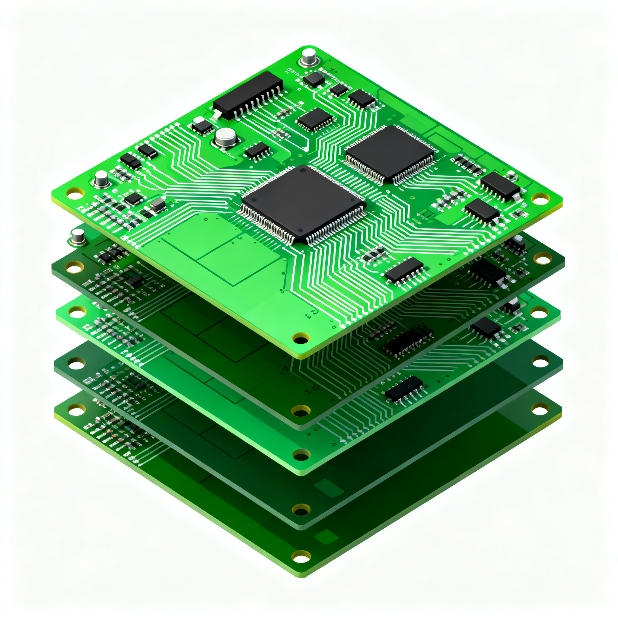
Mastering 4-Layer PCB Stack-Up Optimization: Common Pitfalls and Best Practices for 2026
Mastering 4-Layer PCB Stack-Up Optimization: Common Pitfalls and Best Practices for 2026 table { border-collapse: collapse; width: 100%; margin: 20px 0; } th, td { border: 1px solid #ddd; padding: 8px...
Introduction
The rise of complex electronic devices has necessitated advancements in printed circuit board (PCB) technology. As we approach 2026, optimizing 4-layer PCB stack-ups has become crucial for achieving superior performance, reliability, and cost-efficiency. This article delves into the intricacies of 4-layer PCB stack-up optimization, highlighting common pitfalls and best practices, with a focus on component specifications, datasheets, selection criteria, and application circuits.
Technical Overview
At the heart of modern electronics, the PCB serves as the foundational platform for component interconnection. A 4-layer stack-up typically consists of two signal layers and two power/ground planes. This configuration offers improved electromagnetic compatibility (EMC), reduced signal interference, and better thermal management. The architecture facilitates efficient routing for high-density components, making it ideal for applications in consumer electronics, telecommunications, and automotive industries.
Understanding the principles of stack-up design is essential for engineers. Key concepts include the arrangement of layers, dielectric material selection, and impedance control. Proper layer sequencing minimizes crosstalk and enhances signal integrity. Additionally, selecting appropriate materials and maintaining precise trace widths are critical for achieving desired electrical characteristics.
Detailed Specifications
When designing a 4-layer PCB, understanding the core specifications of integrated circuits (ICs) is paramount. These specifications, often detailed in datasheets, encompass various parameters such as CPU speed, memory capacity, peripheral interfaces, power requirements, and packaging options. Selecting components that align with the intended application ensures optimal performance and reliability.
| Specification | Parameter | Description |
|---|---|---|
| CPU Speed | 1.5 GHz | High-performance processing capability |
| Memory | 4GB DDR4 | Ample storage for data processing |
| Peripherals | USB, I2C, SPI | Versatile interfacing options |
| Power Supply | 3.3V - 5V | Wide range for flexibility |
| Package Type | LQFP | Low-profile and compact design |
| Operating Temperature | -40°C to 85°C | Suitable for industrial applications |
| Clock Speed | 200 MHz | Efficient timing control |
| Communication Ports | Ethernet, CAN | Enhanced connectivity |
| GPIO Pins | 32 | Multiple input/output options |
| Package Size | 10mm x 10mm | Space-saving footprint |
Key Takeaways from the Specifications
The specifications outlined in Table 1 provide a comprehensive view of the IC's capabilities. The 1.5 GHz CPU speed and 4GB DDR4 memory highlight the component's suitability for high-performance applications. The presence of versatile peripherals such as USB, I2C, and SPI ensures broad interfacing potential. Notably, the power supply range of 3.3V to 5V offers flexibility, accommodating various power sources. Designers should consider these parameters to align component selection with application requirements, ensuring optimal functionality and efficiency.
| Characteristic | Value | Description |
|---|---|---|
| Operating Voltage | 3.3V | Standard logic level voltage |
| Max Current | 500mA | Peak current capacity |
| Input Voltage Range | 2.7V - 5.5V | Flexibility in power input |
| Output Voltage | 3.3V | Stable regulated output |
| Input Capacitance | 10pF | Low input load capacitance |
| Output Capacitance | 20pF | Output stability |
| Propagation Delay | 5ns | Fast signal transmission |
| Rise Time | 2ns | Quick signal rise |
| Fall Time | 2ns | Rapid signal fall |
| I/O Voltage Levels | 1.8V - 3.3V | Compatibility with various logic levels |
| Thermal Resistance | 30°C/W | Efficient heat dissipation |
Practical Implications
The electrical characteristics in Table 2 are critical for ensuring reliable circuit operation. The operating voltage of 3.3V aligns with common logic levels, facilitating integration with other components. The maximum current rating of 500mA supports moderate power demands. Fast propagation delay and rise/fall times enable quick signal transitions, essential for high-speed applications. Designers must ensure that these electrical parameters meet the specific needs of their application to maintain functionality and prevent component failure.
| Application | Configuration | Benefits |
|---|---|---|
| Consumer Electronics | Standard 4-layer | Cost-effective and compact |
| Automotive Systems | Enhanced EMC | Improved reliability and safety |
| Telecommunications | High-speed data | Efficient data handling |
| Industrial Automation | Robust design | Durability in harsh environments |
| Medical Devices | Precision circuitry | Accurate and reliable operation |
| Aerospace | Lightweight materials | Weight reduction and performance |
Application Guidelines
The application comparison in Table 3 illustrates the versatility of 4-layer PCBs across various industries. For consumer electronics, the standard 4-layer configuration offers a balance between cost and performance. In automotive systems, enhanced electromagnetic compatibility ensures safety and reliability. Telecommunications benefit from high-speed data handling capabilities, while industrial automation requires robust designs for durability. Selecting the appropriate configuration based on application needs is crucial for achieving optimal results.
Design Considerations
Designing a 4-layer PCB requires careful consideration of several factors to ensure optimal performance and reliability. Key design guidelines include:
- Layer Arrangement: Proper sequencing of signal and power/ground layers minimizes crosstalk and enhances signal integrity.
- Material Selection: Choosing suitable dielectric materials affects thermal management, impedance control, and overall board performance.
- Trace Width and Spacing: Maintaining precise trace widths and spacing is critical for signal integrity and avoiding short circuits.
- Via Design: Optimizing via placement and size reduces signal loss and improves electrical performance.
- Thermal Management: Incorporating thermal vias and heat sinks ensures efficient heat dissipation, preventing overheating.
- EMC Considerations: Implementing shielding techniques and proper grounding reduces electromagnetic interference.
- Design for Manufacturability (DFM): Adhering to manufacturing guidelines ensures cost-effective production and assembly.
Step-by-Step Implementation
Implementing a 4-layer PCB design involves several critical steps:
- Define Requirements: Begin by clearly defining the project requirements, including electrical, mechanical, and environmental specifications.
- Component Selection: Choose components based on performance requirements, availability, and cost. Refer to datasheets for detailed specifications.
- Layer Stack-Up Design: Determine the optimal layer arrangement to balance signal integrity, power distribution, and EMC.
- Schematic Capture: Create a detailed schematic diagram, ensuring correct component placement and connections.
- PCB Layout Design: Use PCB design software to arrange components and route traces, adhering to design guidelines.
- Signal Integrity Analysis: Perform simulations to assess signal integrity and identify potential issues.
- Design Rule Check (DRC): Conduct a DRC to ensure compliance with design rules and manufacturing capabilities.
- Prototype and Testing: Manufacture a prototype and perform thorough testing to validate the design.
Common Issues & Solutions
Designing and manufacturing 4-layer PCBs can present several challenges. Here are some common issues and their solutions:
- Crosstalk: Poor layer arrangement can lead to signal interference. Solution: Optimize layer sequencing and incorporate ground planes.
- Impedance Mismatch: Inadequate trace width and spacing can cause impedance issues. Solution: Use controlled impedance design techniques.
- Thermal Management: Overheating can degrade performance. Solution: Implement thermal vias and heat sinks for efficient heat dissipation.
- Electromagnetic Interference (EMI): Lack of shielding can lead to EMI problems. Solution: Use proper grounding and shielding techniques.
- Manufacturing Defects: Design errors can lead to production issues. Solution: Conduct thorough DRC and adhere to manufacturing guidelines.
Applications & Use Cases
4-layer PCBs are widely used across various industries due to their versatility and performance benefits. Key applications include:
- Consumer Electronics: Smartphones, tablets, and wearable devices utilize 4-layer PCBs for compact and efficient designs.
- Automotive Systems: Advanced driver-assistance systems (ADAS) and in-vehicle infotainment systems rely on 4-layer PCBs for reliable performance.
- Telecommunications: Network equipment and communication devices benefit from high-speed signal processing capabilities.
- Medical Devices: Diagnostic equipment and monitoring devices require precision and reliability provided by 4-layer PCBs.
- Aerospace: Avionics systems use lightweight and durable 4-layer PCBs to withstand extreme conditions.
Selection & Sourcing Guide
Selecting the right components for a 4-layer PCB design involves careful consideration of specifications, availability, and cost. Engineers can access a wide range of components through online platforms such as IC Online. This resource provides comprehensive datasheets, selection criteria, and sourcing options, enabling designers to make informed decisions and streamline the procurement process.
FAQ
Here are some frequently asked questions about 4-layer PCB stack-up optimization:
- What is the primary advantage of a 4-layer PCB? The primary advantage is improved signal integrity and reduced electromagnetic interference due to dedicated power and ground planes.
- How does layer arrangement affect PCB performance? Proper layer arrangement minimizes crosstalk, enhances signal integrity, and improves thermal management.
- What materials are commonly used for 4-layer PCBs? Common materials include FR-4, Rogers, and polyimide, each offering different thermal and electrical properties.
- How can I ensure reliable thermal management? Implementing thermal vias, heat sinks, and appropriate material selection are key to effective thermal management.
- What are the challenges of designing a 4-layer PCB? Challenges include managing signal integrity, preventing EMI, and ensuring manufacturability within budget constraints.
- How can I improve EMC in my PCB design? Techniques include using ground planes, proper trace routing, and incorporating shielding components.
- What tools are available for PCB design? Popular PCB design tools include Altium Designer, Eagle, and KiCad, offering comprehensive design and simulation capabilities.
- How does the choice of ICs impact PCB design? IC specifications influence power distribution, signal routing, and overall board layout, affecting performance and reliability.
- What is the importance of controlled impedance in PCB design? Controlled impedance ensures consistent signal transmission, critical for high-speed applications.
- How do I select the right components for my PCB? Consider factors such as performance requirements, compatibility, cost, and availability, referring to datasheets for detailed specifications.
Conclusion
Mastering 4-layer PCB stack-up optimization is essential for engineers aiming to deliver high-performance, reliable, and cost-effective electronic solutions. By understanding core specifications, electrical characteristics, and application guidelines, designers can make informed decisions that enhance product functionality. With careful consideration of design principles and practical implementation steps, engineers can overcome challenges and achieve successful outcomes in diverse applications.