Investing Smart: The Best PCB Assembly Equipment for Cost-Effective Production
Investing Smart: The Best PCB Assembly Equipment for Cost-Effective Production Introduction In the rapidly evolving electronics industry, the demand for high-quality, cost-effective printed circuit bo...
Introduction
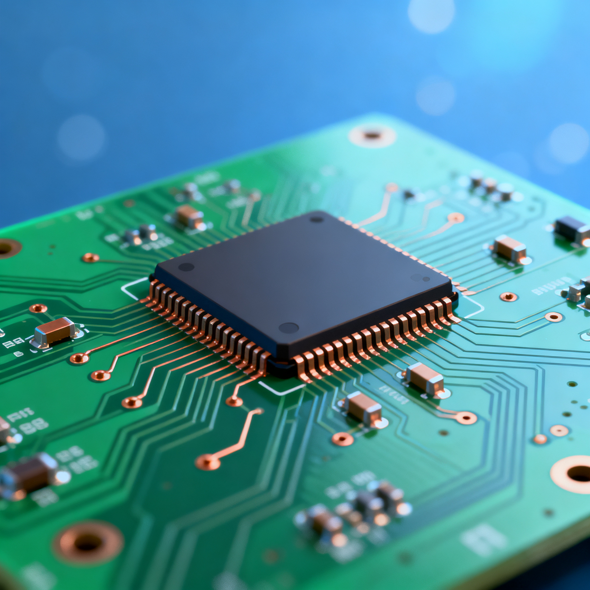
In the rapidly evolving electronics industry, the demand for high-quality, cost-effective printed circuit board (PCB) assembly is at an all-time high. PCBs are the backbone of electronic devices, making their design and assembly crucial for manufacturing success. This article explores the best PCB assembly equipment and practices to ensure efficient production without compromising on quality. By adhering to industry standards and leveraging advanced technologies, manufacturers can optimize their PCB designs and streamline the assembly process, ultimately leading to reduced costs and enhanced product performance.
Technical Overview
PCB assembly involves several critical steps, from designing the layout to assembling the components. Core concepts include understanding PCB layout rules, stackup design, signal integrity, and manufacturing considerations. The architecture of PCBs typically involves multiple layers that can be customized based on the application's requirements. Signal integrity is a key factor, as it ensures the reliable transmission of electrical signals across the board. Adhering to industry standards such as IPC-A-610 and IPC-2221 provides guidelines for quality and reliability. Advanced assembly equipment and techniques, including automated pick-and-place machines and reflow soldering, are integral to achieving high-precision manufacturing.
Detailed Specifications
When it comes to PCB design and assembly, understanding the specifications is crucial. Specifications such as trace width, spacing, via sizes, and clearances play a significant role in determining the board's performance and reliability. These parameters ensure that electrical signals are transmitted efficiently and that the board can withstand environmental stresses. The following table outlines key PCB design rules, providing a foundation for cost-effective and high-quality production.
| Design Parameter | Minimum Value | Recommended Value |
|---|---|---|
| Trace Width | 0.15 mm | 0.20 mm |
| Trace Spacing | 0.15 mm | 0.20 mm |
| Via Diameter | 0.30 mm | 0.50 mm |
| Pad Clearance | 0.20 mm | 0.25 mm |
| Drill Hole Size | 0.20 mm | 0.30 mm |
| Solder Mask Clearance | 0.10 mm | 0.15 mm |
| Component Clearance | 0.50 mm | 1.00 mm |
| Edge Clearance | 0.50 mm | 1.00 mm |
| Silkscreen Clearance | 0.10 mm | 0.15 mm |
| Aspect Ratio | 6:1 | 8:1 |
Key Takeaways from the Specifications
The specifications outlined in the table are essential for ensuring the functional and structural integrity of PCBs. Trace width and spacing are critical for current carrying capacity and signal integrity. Adequate pad clearance and drill hole sizes ensure reliable solder joints and component placement. Adhering to these parameters helps in minimizing electromagnetic interference and ensures that the board can handle the required electrical loads. Proper design specifications also contribute to the manufacturability of the PCB, reducing the likelihood of errors during assembly and increasing yield rates.
| Layer Configuration | Description | Applications |
|---|---|---|
| 2-Layer | Basic configuration with top and bottom layers | Simple circuits, low-density applications |
| 4-Layer | Includes two internal planes for power and ground | Moderate complexity, improved EMI performance |
| 6-Layer | Four signal layers with two planes for power and ground | High-speed circuits, enhanced signal integrity |
| 8-Layer | Six signal layers with two dedicated planes | Complex circuits, high-density applications |
| 10-Layer | Eight signal layers with two planes for power and ground | Advanced RF applications, superior EMI control |
| 12-Layer | Ten signal layers with two internal planes | High-performance computing, data centers |
Practical Implications
Layer stackup configurations are pivotal in determining the PCB's performance in various applications. A 2-layer board is cost-effective for simple circuits, while a 4-layer configuration provides improved EMI performance. For high-speed circuits, a 6-layer stackup enhances signal integrity by offering additional routing layers and dedicated power planes. As complexity increases, using an 8-layer or 10-layer stackup can accommodate more components and maintain signal integrity in high-density applications. Understanding the appropriate layer configuration is crucial for balancing performance, cost, and manufacturability in PCB design.
| Material | Dielectric Constant (Dk) | Loss Tangent (Df) |
|---|---|---|
| FR-4 | 4.5 | 0.02 |
| Rogers 4350B | 3.66 | 0.0037 |
| Rogers 5880 | 2.20 | 0.0009 |
| Isola IS620 | 3.45 | 0.002 |
| Arlon 85N | 3.5 | 0.003 |
| Nelco N4000-13 | 3.7 | 0.009 |
| Megtron 6 | 3.5 | 0.002 |
| PTFE | 2.1 | 0.001 |
| Polyimide | 3.4 | 0.004 |
Application Guidelines
The choice of PCB material significantly affects the board's electrical performance. FR-4 is a cost-effective material suitable for general applications, but for high-frequency applications, materials like Rogers 4350B and 5880 offer lower dielectric constants and loss tangents, providing superior signal integrity and reduced signal loss. Advanced materials such as Megtron 6 and PTFE are ideal for RF applications due to their excellent electrical properties. Selecting the right material involves considering factors like operating frequency, thermal stability, and cost, ensuring that the PCB meets the specific requirements of the application.
Design Considerations
When designing PCBs, several considerations must be addressed to ensure optimal performance and manufacturability. First, adhere to industry design rules for trace width, spacing, and via sizes to maintain signal integrity and prevent crosstalk. Proper layer stackup configuration is crucial for managing electromagnetic interference and supporting high-speed signals. Material selection should align with the application's frequency and environmental conditions, balancing performance and cost. Additionally, thermal management is vital, especially in high-power applications, to prevent overheating and ensure reliability. Incorporating design for manufacturability (DFM) principles can reduce production costs and improve yield by simplifying assembly processes and minimizing errors.
Step-by-Step Implementation
- Define Requirements: Begin by clearly defining the PCB's functional and performance requirements, including electrical, mechanical, and environmental specifications.
- Create Schematic: Develop a detailed schematic diagram, specifying all components and their connections, ensuring it aligns with the defined requirements.
- Design PCB Layout: Use PCB design software to create the layout, adhering to design rules for trace widths, spacing, and clearances. Optimize the layout for signal integrity and manufacturability.
- Select Materials: Choose appropriate materials based on electrical performance, thermal properties, and cost considerations. Ensure compatibility with the application's operating conditions.
- Define Layer Stackup: Determine the optimal layer stackup configuration to support the circuit's complexity and signal requirements, balancing cost and performance.
- Perform Simulations: Conduct signal integrity and thermal simulations to validate the design, identifying and mitigating potential issues before fabrication.
- Prototype and Test: Fabricate a prototype PCB and perform thorough testing to verify functionality, performance, and compliance with specifications.
- Refine and Finalize: Analyze test results, refine the design as needed, and finalize the PCB for mass production, ensuring all documentation is complete.
Common Issues & Solutions
- Signal Integrity Problems: Use proper trace impedance matching and minimize loop areas to prevent reflections and crosstalk.
- Thermal Management Challenges: Implement heat sinks, thermal vias, and adequate copper planes to dissipate heat effectively.
- Component Misalignment: Utilize automated pick-and-place machines and accurate component libraries to ensure precise placement.
- Solder Joint Failures: Optimize reflow profiles and use quality solder paste to achieve reliable solder joints.
- Electromagnetic Interference (EMI): Design with proper grounding, shielding, and use of ferrite beads to minimize EMI.
- Manufacturability Issues: Apply DFM principles to simplify assembly processes and reduce the likelihood of errors during production.
Applications & Use Cases
PCBs are ubiquitous in electronic devices, serving as the foundation for applications ranging from consumer electronics to industrial machinery. In consumer electronics, PCBs are used in smartphones, tablets, and wearable devices, where compact size and high performance are essential. In industrial applications, PCBs are integral to control systems, robotics, and automation equipment, where reliability and durability are paramount. The automotive industry relies on PCBs for advanced driver-assistance systems (ADAS) and infotainment systems, requiring robust designs to withstand harsh environments. Additionally, in telecommunications, PCBs are critical for networking equipment and high-frequency applications, demanding superior signal integrity and thermal management.
Selection & Sourcing Guide
When selecting PCB assembly equipment and materials, consider factors such as production volume, complexity, and cost. It's essential to source components and materials from reputable suppliers to ensure quality and reliability. For comprehensive sourcing options, visit IC Online, a trusted platform for electronic components and materials. Evaluate suppliers based on their compliance with industry standards, lead times, and technical support capabilities to make informed decisions that align with your production needs.
FAQ
- What are the key factors to consider when designing a PCB? Key factors include trace width and spacing, layer stackup, material selection, and thermal management.
- How does layer stackup affect PCB performance? Layer stackup influences signal integrity, EMI performance, and the board's ability to support high-density routing.
- Why is material selection important in PCB design? Material selection impacts electrical performance, thermal stability, and cost, influencing the overall functionality and reliability of the PCB.
- What is the role of IPC standards in PCB design? IPC standards provide guidelines for design, assembly, and quality inspection, ensuring reliability and compliance with industry practices.
- How can signal integrity be improved in PCB designs? Improve signal integrity through proper trace impedance matching, minimizing loop areas, and using differential signaling.
- What are common thermal management techniques for PCBs? Techniques include using heat sinks, thermal vias, copper planes, and appropriate material selection.
- How do you ensure manufacturability in PCB design? Apply DFM principles, simplify assembly processes, and optimize design for automated manufacturing equipment.
- What are the benefits of using advanced PCB assembly equipment? Advanced equipment enhances precision, reduces assembly time, and improves yield rates, leading to cost-effective production.
- How can EMI be minimized in PCB designs? Minimize EMI by designing proper grounding, using shielding, and incorporating ferrite beads in critical areas.
- What is the significance of prototype testing in PCB design? Prototype testing validates functionality, identifies potential issues, and ensures compliance with design specifications before mass production.
Conclusion
Investing in the right PCB assembly equipment and adhering to best practices in design and manufacturing are crucial for achieving cost-effective production. By understanding and implementing key design rules, layer stackup configurations, and material properties, manufacturers can optimize their PCB designs for performance and reliability. Leveraging advanced assembly technologies and adhering to industry standards ensures high-quality outcomes, ultimately leading to successful product development and competitive advantages in the electronics market.