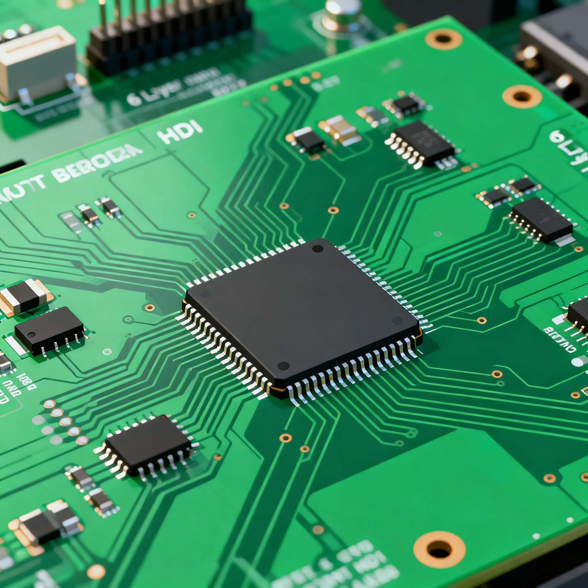
Industrial IoT PCB Manufacturing in 2026: Best Practices for High-Reliability 6-Layer HDI Boards
Why 6‑Layer HDI Is Becoming the Baseline for Rugged IIoT Edge Nodes Industrial IoT edge nodes are no longer simple sensor translators. Today’s designs pack multi‑core Arm® processors, FPGA co‑processo...
Why 6‑Layer HDI Is Becoming the Baseline for Rugged IIoT Edge Nodes
Industrial IoT edge nodes are no longer simple sensor translators. Today’s designs pack multi‑core Arm® processors, FPGA co‑processors, and high‑speed DDR4 memory interfaces into enclosures that must survive −40°C cold starts, condensing humidity, and vibration levels that would shake a 4‑layer board to failure. At the same time, mechanical footprints are shrinking — a smart motor controller that once filled a DIN‑rail box now fits in a palm‑sized IP67 housing. These two forces, performance density and environmental stress, are pushing 6‑layer HDI from a niche luxury to the practical baseline for rugged IIoT products.
When you route a 0.5 mm pitch BGA on a conventional 4‑layer through‑hole board, you quickly run out of escape routing channels. The larger drill diameters required for through‑vias consume valuable real estate, forcing you to add layers or abandon impedance control on critical nets. A 6‑layer HDI stackup with laser‑drilled microvias changes the equation: blind vias in the outer layers free inner‑layer routing channels, while buried vias connect internal planes without breaking the reference continuity that high‑speed signals demand. The result is a board that can fan out a 400‑ball FPGA, maintain 50 Ω single‑ended and 100 Ω differential impedances, and still leave room for isolated power islands — all within a 50 × 70 mm outline.
Reliability requirements add another layer of justification. Industrial IoT devices are often installed in remote locations — wind turbine nacelles, oilfield pump jacks, or outdoor telemetry cabinets — where service calls are expensive. The IPC‑2221 design standard (IPC‑2221, Generic Standard on Printed Board Design) emphasizes that conductor spacing, via aspect ratios, and dielectric selection must account for the full operating environment, not just the bench. 6‑layer HDI boards, when built to IPC Class 3 acceptance criteria, deliver the via integrity and insulation resistance needed to survive thousands of thermal cycles without barrel cracking or CAF (Conductive Anodic Filament) growth. This isn’t about over‑engineering; it’s about matching the board architecture to the lifetime cost of field failures.
Key Takeaway: If your IIoT design includes a BGA with 0.8 mm pitch or finer, a high‑speed memory bus, or a requirement for 10‑year service life in an unheated enclosure, a 6‑layer HDI board is no longer optional — it’s the starting point for a reliable, manufacturable product.
Stackup Architecture and Signal Integrity Essentials for 6‑Layer HDI IIoT Boards
A well‑designed 6‑layer HDI stackup does more than squeeze traces between planes. It creates a controlled electromagnetic environment where return currents flow directly beneath their signals, crosstalk stays below 2%, and power delivery networks exhibit low impedance out to several hundred MHz. The most common configuration for IIoT boards is a 1‑2‑1 stackup: one microvia layer on top, a two‑layer core with buried vias, and one microvia layer on the bottom. This structure provides four routing layers (L1, L3, L4, L6) with two solid reference planes (L2 and L5) and requires only a single sequential lamination cycle, keeping cost and thermal stress manageable.
For designs that must route DDR4 or Gigabit Ethernet, the layer assignment shown in the table below has proven effective. High‑speed signals on L1 and L6 are immediately adjacent to ground planes, minimizing loop inductance. L3 and L4 are sandwiched between ground and power, creating a stripline environment that naturally suppresses far‑end crosstalk. The buried vias connecting L2–L5 can be drilled with a larger diameter (0.2–0.25 mm) because they don’t consume outer‑layer real estate, improving plating uniformity and long‑term reliability.
| Layer | Assignment | Dielectric Thickness (µm) | Copper Weight (oz) | Via Type | Impedance Control |
|---|---|---|---|---|---|
| L1 (Top) | Signal (high‑speed) | Prepreg 60–80 | 0.5 | Laser microvia to L2 | 50 Ω SE / 100 Ω diff |
| L2 | Ground plane | Core 100–150 | 1.0 | Buried via to L5 | Reference plane |
| L3 | Signal (stripline) | Prepreg 100–120 | 0.5 | Buried via to L4 (optional) | 50 Ω SE |
| L4 | Power plane | Core 100–150 | 1.0 | Buried via to L3 | PDN target < 0.1 Ω |
| L5 | Ground plane | Prepreg 60–80 | 1.0 | Buried via to L2 | Reference plane |
| L6 (Bottom) | Signal (high‑speed) | — | 0.5 | Laser microvia to L5 | 50 Ω SE / 100 Ω diff |
Impedance tolerances of ±10% are achievable with this stackup when fabricators use tightly controlled dielectric constants and etch processes. For gigabit interfaces, some engineers tighten the specification to ±7% on differential pairs, which requires additional process monitoring but is well within the capability of an experienced HDI shop. All via structures must meet the IPC‑A‑610 Class 3 criteria (IPC‑A‑610, Acceptability of Electronic Assemblies): minimum annular ring of 25 µm for laser vias, plating thickness ≥20 µm in the barrel, and no voids larger than 5% of the via diameter. Cross‑section analysis of first‑article boards is the only way to verify these parameters before committing to production volumes.
Tip: When specifying a 1‑2‑1 stackup, ask your fabricator to provide a detailed impedance coupon report that includes both single‑ended and differential test traces on L1, L3, L4, and L6. Variations in prepreg flow during lamination can shift impedance on inner layers by 3–5 Ω, so coupon data from the actual panel is far more valuable than a simulation snapshot.
6‑Layer HDI vs. Conventional Multilayer: When the Extra Density Pays Off in IIoT
Not every industrial IoT board needs HDI. A simple Modbus gateway with a low‑pin‑count microcontroller and a handful of discrete components can be built reliably on a 4‑layer through‑hole board. But once you add a wireless SoC with integrated antenna tuning, isolated CAN transceivers, and a power‑over‑Ethernet front‑end, the routing density quickly pushes a 4‑layer design into long, meandering traces that degrade signal quality and increase EMI susceptibility. The comparison below helps you decide where the break‑even point lies for your specific design.
| Comparison Metric | 4‑Layer Through‑Hole | 6‑Layer HDI (1‑2‑1) | 8‑Layer HDI (2‑4‑2) | Selection Criteria & Failure Boundary |
|---|---|---|---|---|
| Minimum BGA pitch supported | 0.8 mm (with dog‑bone fanout) | 0.5 mm (via‑in‑pad with filled vias) | 0.4 mm (stacked microvias) | Choose 6‑layer HDI for 0.5–0.65 mm pitch; 8‑layer only when 0.4 mm pitch or >800 I/Os required. |
| Signal integrity (crosstalk) | −15 dB typical (aggressor‑victim spacing limited) | −25 dB or better (adjacent ground planes) | −30 dB (additional routing channels) | For 1 Gbps Ethernet or DDR3+, 6‑layer HDI is the minimum to meet eye‑diagram masks. |
| Thermal management | Limited copper area for heat spreading | Solid inner planes act as heat spreaders | Multiple power/ground plane pairs improve thermal vias | If board must dissipate >5 W without a heatsink, 6‑layer HDI with thermal via arrays is recommended. |
| Board real estate efficiency | 60–70% utilization (through‑vias block routing) | 85–90% utilization (microvias free outer layers) | >90% utilization | When PCB outline is fixed and component density exceeds 25 parts/cm², HDI pays for itself by avoiding a larger enclosure. |
| Relative cost at 1k volume | 1.0× (baseline) | 1.6–2.0× | 2.5–3.5× | The cost premium for 6‑layer HDI is often offset by eliminating connectors or reducing layer count from a non‑HDI 8‑layer board. |
| Reliability in thermal cycling (−40 to +125°C) | Through‑via barrels at risk of cracking after 500 cycles | Microvias survive >1000 cycles when aspect ratio ≤1:1 | Stacked microvias require careful material matching to survive 1000 cycles | For 10‑year outdoor IIoT, 6‑layer HDI with staggered microvias offers the best reliability‑to‑cost ratio. |
Note: Nova PCBA’s HDI manufacturing line (Nova PCBA HDI PCB services) supports all three stackup types — 4‑layer through‑hole, 6‑layer HDI, and 8‑layer HDI — giving you the flexibility to choose the architecture that matches your density and reliability requirements without being forced into a one‑size‑fits‑all solution.
The cost comparison deserves a closer look. A 6‑layer HDI board typically costs 60–100% more than a 4‑layer through‑hole board of the same dimensions. But if that 4‑layer board requires an extra 20 mm of board length to complete routing, or forces you to use a larger connector to break out signals, the total system cost may actually be higher. Many IIoT teams find that moving to 6‑layer HDI lets them eliminate a mezzanine connector or consolidate two boards into one, delivering a net cost reduction at the product level. The key is to evaluate cost at the system level, not just the bare board price.
Specifying and Sourcing High‑Reliability 6‑Layer HDI for Industrial Environments
Getting a 6‑layer HDI board that survives a decade in a condensing enclosure starts long before you send Gerber files to a fabricator. It begins with laminate selection, via geometry decisions, and a clear test specification that goes beyond basic electrical continuity. The following guidance addresses the most common failure modes we see in IIoT programs and how to avoid them.
Laminate selection: the foundation of CAF resistance. In high‑humidity environments with DC bias voltages, moisture can wick along glass‑fiber bundles and form conductive filaments between adjacent plated holes — a phenomenon known as Conductive Anodic Filament (CAF). Standard FR‑4 with a low Tg (130°C) and ordinary E‑glass is particularly susceptible. The table below compares laminates commonly used in industrial HDI boards, ranked by their resistance to CAF and delamination.
| Laminate Type | Tg (°C) | Z‑Axis CTE (ppm/°C) | CAF Resistance | Moisture Absorption (%) | Relative Cost | Best Application |
|---|---|---|---|---|---|---|
| Standard FR‑4 | 130–140 | 50–70 (above Tg) | Low | 0.15–0.20 | 1.0× | Indoor, non‑condensing |
| High‑Tg FR‑4 (170–180°C) | 170–180 | 35–45 | Moderate (with CAF‑resistant glass) | 0.12–0.15 | 1.2–1.4× | Most IIoT edge nodes; specify CAF‑resistant weave |
| Halogen‑free Mid‑Tg | 150–160 | 40–50 | Good (inherently lower ionic contamination) | 0.10–0.12 | 1.5–1.8× | Outdoor enclosures with occasional condensation |
| Polyimide | 250+ | 20–30 | Excellent | 0.08–0.10 | 3.0–4.0× | Extreme condensation, down‑hole, or continuous 125°C operation |
For most IIoT applications — a smart factory sensor hub, a remote telemetry unit, or an outdoor lighting controller — high‑Tg FR‑4 with a CAF‑resistant glass weave (often marketed as “CAF‑resistant” or “anti‑CAF” by laminate suppliers) provides the right balance of reliability and cost. Reserve polyimide for designs that face continuous high humidity with DC bias, such as submersible pump controllers or geothermal instrumentation.
Microvia aspect ratios: the reliability sweet spot. Laser‑drilled microvias in a 1‑2‑1 stackup typically have a diameter of 0.1–0.15 mm and a dielectric thickness of 60–80 µm, yielding an aspect ratio of 0.8:1 to 1:1. This is the range where plating quality is most consistent and thermal cycle survival exceeds 1000 cycles. Pushing the aspect ratio to 1.2:1 is possible with advanced laser processing and thin, uniform prepregs, but the risk of plating voids and barrel cracks increases. For IIoT designs that must endure wide temperature swings, we recommend staying at or below 1:1. If your BGA escape requires deeper vias, consider a 2‑2‑2 stackup with stacked microvias rather than forcing a single deep microvia.
Testing beyond electrical test: IST and HATS. A flying‑probe continuity test tells you the board is good today; Interconnect Stress Testing (IST) or Highly Accelerated Thermal Shock (HATS) tells you it will still be good after five years of sunrise‑to‑sunset thermal cycling. These methods heat and cool test coupons repeatedly while monitoring resistance changes in via chains. A resistance increase of more than 10% indicates a developing crack or interfacial separation. Specify IST or HATS on every production lot for Class 3 IIoT boards, and require the fabricator to provide coupon data with each shipment. This is not an exotic request — it’s standard practice for high‑reliability HDI suppliers.
DFM pitfalls that delay IIoT programs. Several design decisions can turn a straightforward 6‑layer HDI build into a protracted engineering exercise:
- Stacked microvias without a clear reliability justification. Stacked vias require precise registration and a second lamination cycle, adding cost and thermal stress. Use staggered microvias wherever possible.
- Via‑in‑pad without specifying filled and capped vias. An open via in a BGA pad will wick solder away from the joint, causing head‑in‑pillow defects. Always specify conductive or non‑conductive via fill with a planar copper cap for via‑in‑pad structures.
- Mixed dielectric materials in a single stackup. Combining high‑Tg FR‑4 with a low‑loss RF prepreg on the same board can cause warpage during reflow if the CTE mismatch isn’t modeled. Stick to a single laminate family unless you’ve run a thermal simulation.
- Insufficient copper in buried via barrels. Buried vias that connect L2–L5 may see high DC currents in power distribution networks. Specify a minimum plating thickness of 25 µm and verify it with cross‑section analysis.
When vetting a fabricator, ask for evidence of IPC Class 3 HDI production volume — not just a certificate on the wall, but recent first‑article reports and IST data from jobs similar to yours. A shop that primarily builds consumer electronics may struggle with the process controls required for industrial reliability. Nova PCBA’s engineering team (Nova PCBA assembly services) routinely reviews stackup designs and provides DFM feedback before tooling begins, helping you catch these issues early and keep your IIoT program on schedule.
Your Toughest Questions About 6‑Layer HDI for IIoT, Answered
Q: What minimum via aspect ratio can I reliably achieve on a 6‑layer HDI board with 0.5 mm pitch BGAs?
For a typical 1‑2‑1 stackup using laser‑drilled microvias, aspect ratios of 0.8:1 to 1:1 are standard. With advanced laser processing and thin dielectrics, some fabricators can push to 1.2:1, but staying ≤1:1 improves yield and long‑term reliability in thermal cycling. For a 0.5 mm pitch BGA, a 0.1 mm via in a 70 µm dielectric gives an aspect ratio of 0.7:1 — well within the safe zone — and allows a 0.25 mm capture pad with adequate solder mask clearance.
Q: How do I qualify a PCB fabricator for IPC Class 3 6‑layer HDI in an IIoT program?
Request evidence of Class 3 HDI production volume, ask for microvia reliability test data (IST or HATS coupons), verify in‑process inspection capabilities for via plating thickness and voiding, and conduct a first‑article cross‑section analysis against IPC‑A‑610 Class 3 criteria. A reputable fabricator will provide a qualification package that includes cross‑section micrographs of via structures, plating thickness measurements, and IST results from a recent production lot. If they hesitate or offer only a certificate of conformance, look elsewhere.
Q: What are realistic lead times for 6‑layer HDI prototypes and production in 2026?
Prototype turns of 5–10 days are achievable from quick‑turn HDI specialists, while production batches typically run 3–5 weeks. Lead times stretch when using exotic laminates or sequential lamination steps beyond 2‑2‑2, so early material selection is critical. If your program timeline is tight, lock in the laminate choice during the design phase and ask your fabricator to reserve material before the Gerber files are final.
Q: Which laminate materials best resist CAF and delamination in high‑humidity IIoT installations?
High‑Tg FR‑4 (170–180°C) with CAF‑resistant glass weave is the cost‑effective baseline. For extreme condensation or outdoor enclosures, polyimide or halogen‑free mid‑Tg materials with low Z‑axis expansion offer superior moisture resistance and are worth the premium. The key parameter is the laminate’s moisture absorption rating and its CTE above Tg; materials with Z‑axis CTE below 50 ppm/°C and moisture absorption under 0.15% perform well in condensing environments.
Q: How does sequential lamination affect cost and reliability for a 6‑layer HDI stackup?
Each sequential lamination cycle adds about 15–25% to the bare board cost and introduces additional thermal stress. A 1‑2‑1 stackup (one lamination cycle) is the most economical and reliable; moving to 2‑2‑2 (two cycles) should only be done when routing density absolutely requires stacked microvias. If you can escape your BGA with staggered microvias in a 1‑2‑1 stackup, you’ll get better reliability and a lower cost.
Q: What testing methods beyond standard electrical test prove long‑term reliability of 6‑layer HDI in IIoT?
Interconnect Stress Testing (IST) or Highly Accelerated Thermal Shock (HATS) are the gold standards. These methods repeatedly cycle coupons through high‑temperature gradients to detect latent via barrel cracks and interfacial separation before field deployment. For Class 3 IIoT boards, we recommend IST testing to 300 cycles from ambient to 150°C, with continuous resistance monitoring. A resistance shift of less than 10% after 300 cycles indicates a robust via structure that will survive years of outdoor thermal cycling.
References & Further Reading
- IPC — Association Connecting Electronics Industries
- IPC‑A‑610: Acceptability of Electronic Assemblies
- IPC‑2221: Generic Standard on Printed Board Design
- Nova PCBA — Professional PCB Assembly Services
- Nova PCBA HDI PCB Manufacturing
- Nova PCBA PCB Assembly Capabilities
- Sierra Circuits: HDI PCB Design Guidelines
- EETimes: HDI PCBs for Industrial IoT Reliability Demands
- PCBWay: 6‑Layer HDI PCB Prototype Service
- Ultra Librarian: HDI PCB Design Considerations for Reliability
Choosing the right PCB architecture for an industrial IoT product is a decision that echoes through the entire product lifecycle. A 6‑layer HDI board, properly specified and sourced, gives you the signal integrity, thermal resilience, and long‑term reliability that harsh environments demand — without the cost and complexity of an 8‑layer build. When you’re ready to move from stackup simulation to production, Nova PCBA’s assembly and manufacturing teams can support your program with IPC Class 3 HDI capability, in‑house DFM review, and the testing rigor that keeps IIoT nodes running year after year.